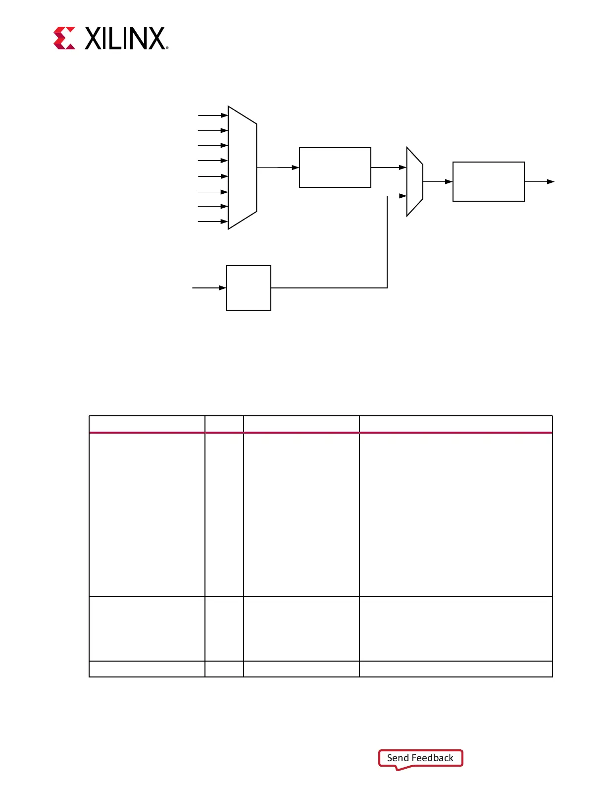
Figure 32: TX Pattern Generator Block
Error
Insertions
FIFO
Polarity
Inversion
PRBS-7
PRBS-9
PRBS-13
PRBS-15
PRBS-23
PRBS-31
Alternating 1'b0 and 1'b1
Square Wave with 64 UI Period
CH0/1_TXDATA
X22032-112618
Ports and Attributes
The following table denes the paern generator ports.
Table 38: Pattern Generator Ports
Port Name Dir Clock Domain Description
CH[0/1]_TXPRBSPTN[3:0] In CH[0/1]_TXUSRCLK2 Transmitter pattern generator control.
4’b0000: Standard operation mode (test
pattern generation is off)
4’b0001: PRBS-7
4’b0010: PRBS-9
4’b0011: PRBS-15
4’b0100: PRBS-23
4’b0101: PRBS-31
4’b0110: PRBS-13
4’b1000: Reserved
4’b1001: Alternating 1b’0 and 1’b1
4’b1010: Square wave with 64 UI period
CH[0/1]_TXPRBSINERR In CH[0/1]_TXUSRCLK2 When this port is driven High, a single error is
forced in the PRBS transmitter for every
CH[0/1]_TXUSRCLK2 clock cycle that the port is
asserted.
When CH[0/1]_TXPRBSPTN is set to 4’b0000, this
port does not affect CH[0/1]_TXDATA.
CH[0/1]_TXQPRBSEN
In CH[0/1]_TXUSRCLK2 Reserved. This port must always be set to 1’b0.
The following table denes the paern generator aribute.
Chapter 3: Transmitter
UG581 (v1.0) January 4, 2019 www.xilinx.com
Virtex UltraScale+ GTM Transceivers 69
 Loading...

