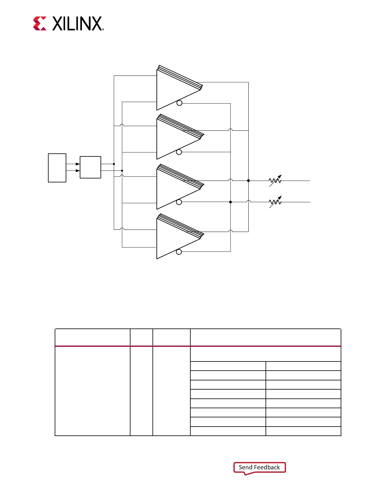
Figure 35: TX Configurable Driver Block Diagram
4-Tap
FIR
PISO
Pre-Emphasis
Pad Driver
Main
Pad Driver
Post-Emphasis
Pad Driver
50Ω
CH0/1_GTMTXP
CH0/1_GTMTXN
CH0/1_TXEMPPRE[4:0]
CH0/1_TXDRVAMP[4:0]
CH0/1_TXEMPPRE2[3:0]
CH0/1_TXEMPPOST[4:0]
Pre-Emphasis 2
Pad Driver
50Ω
X20916-060618
Ports and Attributes
The following table denes the TX congurable driver ports.
Table 46: TX Configurable Driver Ports
Port Dir
Clock
Domain
Description
CH[0/1]_TXDRVAMP[4:0] Input Async Driver swing control. The default is user specified. All listed
values are in mV
PPD
.
[4:0] mV
PPD
5’b00000
250
5’b00001
275
5’b00010
300
5’b00011
325
5’b00100
350
5’b00101
375
5’b00110
400
Chapter 3: Transmitter
UG581 (v1.0) January 4, 2019 www.xilinx.com
Virtex UltraScale+ GTM Transceivers 78
 Loading...

