Table 46: TX Configurable Driver Ports (cont'd)
Port Dir
Clock
Domain
Description
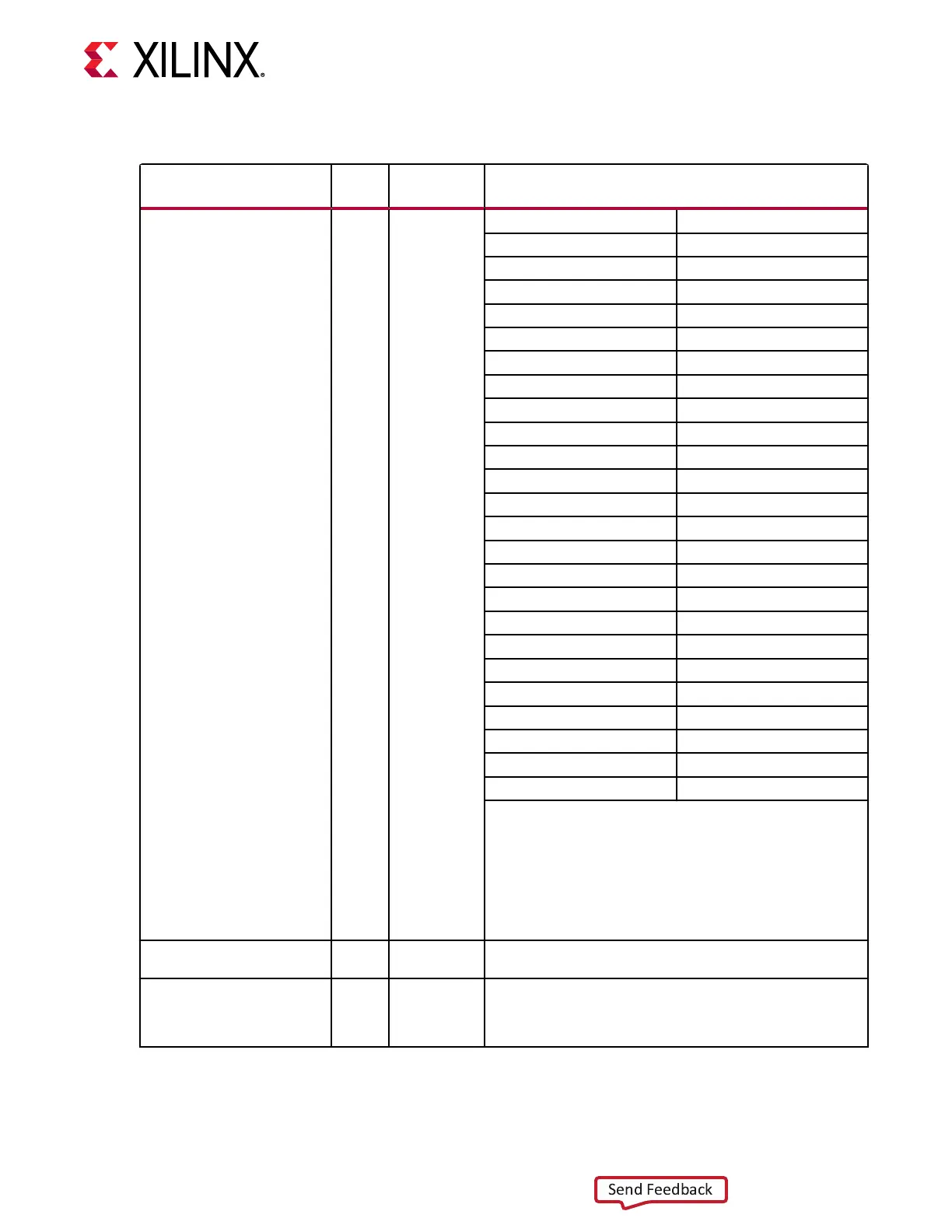
5’b00111
425
5’b01000
450
5’b01001
475
5’b01010
500
5’b01011
525
5’b01100
550
5’b01101
575
5’b01110
600
5’b01111
625
5’b10000
650
5’b10001
675
5’b10010
700
5’b10011
725
5’b10100
750
5’b10101
775
5’b10110
800
5’b10111
825
5’b11000
850
5’b11001
875
5’b11010
900
5’b11011
925
5’b11100
950
5’b11101
975
5’b11110
1000
5’b11111
1025
Notes:
1. The peak-to-peak differential voltage is defined when
CH[0/1]_TXEMPPOST = 5’b00000, CH[0/1]_TXEMPPRE =
5’b00000, and CH[0/1]_TXEMPPRE2 = 4’b0000.
2. For UltraScale+ FPGAs, the output swing described above
is obtained using settings from the Wizard design, and the
recommended values from the Wizard should not be
changed.
CH[0/1]_TXINHIBIT
Input TXUSRCLK2 When High, this signal blocks transmission of CH[0/1]_TXDATA
and forces CH[0/1]_GTMTXP to 0 and CH[0/1]_GTMTXN to 1.
CH[0/1]_TXEMPMAIN[5:0] Input Allows the main cursor coefficients to be directly set if
CH[0/1]_TX_DRV_CFG0[0] attribute is set to 1’b1.
CH[0/1]_TXDRVAMP should be used together with
CH[0/1]_TXEMPMAIN to achieve the desired TX output swing.
Chapter 3: Transmitter
UG581 (v1.0) January 4, 2019 www.xilinx.com
Virtex UltraScale+ GTM Transceivers 79
 Loading...

