Do you have a question about the Yamaha DSP-AX1/RX-V1 and is the answer not in the manual?
Warning about static discharge and how to ground oneself during servicing.
Important reminder to turn off the unit before disassembly and check work before applying power.
Components with special characteristics are marked and must be replaced with identical parts.
Procedure to verify insulation and measure leakage current after service.
Notice regarding lead and other chemical traces in components, with handling precautions.
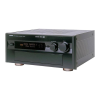
Illustration and identification of controls on the DSP-AX1 front panel.
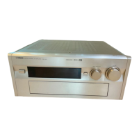
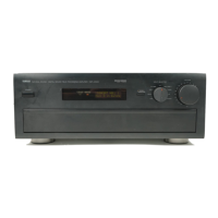
Illustration and identification of controls on the RX-V1 front panel.
Illustration and identification of connectors on the rear panel of DSP-AX1 models.
Illustration and identification of connectors on the rear panel of RX-V1 models.
Detailed specifications for the audio output, input, and tone control sections.
Technical specifications for video signal types, levels, and frequency response.
Specifications for FM reception, including tuning range, sensitivity, and selectivity.
Specifications for AM reception, including tuning range and sensitivity.
General specifications including power supply, consumption, dimensions, and weight.
Diagram showing the physical dimensions of the unit in millimeters and inches.
Table detailing speaker settings and input configurations.
Table showing video signal superimposing connections.
Table detailing parameters like initial delay, room size, and liveness for SP MODE.
Table detailing parameters like initial delay, room size, and liveness for HP MODE.
List of internal components with their corresponding reference numbers and PCB locations.
Instructions for removing the top, bottom, and front panels.
Instructions for removing DSP and Main PCBs by unscrewing panels and frames.
Table listing the 14 DIAG menu items and their corresponding sub-menus.
Table mapping diagnostic menu items to specific remote control key codes.
Procedure to start the DIAG mode for DSP-AX1 and RX-V1 units.
How to start DIAG mode when the protection function is active, to bypass it.
Description of the opening message and DIAG menu display.
Explanation of protection status displays indicating various abnormalities.
Information on how the protection function history is stored and cleared.
Key combinations for selecting DIAG menus and sub-menus.
List of functions available when the DIAG menu is active.
Details of the initial settings applied when starting the DIAG function.
Explanation of the ANALOG BYPASS sub-menu and signal flow.
Description of AC3D2av signal output paths for various sources.
Description of DSP6#1 and DSP6#2 output signal paths.
Explanation of DSP 0dB and FULL BIT sub-menus and signal flow.
Explanation of YSS918/908 and FULL BIT sub-menus and signal passage.
Description of decoder signal paths for different channel sources.
Explanation of 2ch/MULTI and FULL BIT sub-menus and signal paths.
Detailed explanation of the 2ch/MULTI sub-menu, including signal paths.
Explanation of YSS918 Pro Logic and Effect Off sub-menus.
Explanation of YSS908 Pro Logic and Effect Off sub-menus.
Explanation of DECODER and DSP bypass sub-menus and signal paths.
Table of speaker settings and their configurations and applications.
Description of how the FL driver and tube are checked using segment lighting.
Explanation of manual test sub-menus for outputting noise through channels.
Sub-menus to check RS-232C data transmission and flow port operation.
Control of RAM initialization for presets: INHIBIT and RESERVED.
Table showing factory preset FM and AM station data by page and model.
Details on fan operation history and key scanning detection.
Explanation of tuner sensitivity, temperature, and protection detection.
Explanation of IF STATUS bytes indicating communication and signal status.
Detailed information on IF STATUS items 1 through 18.
Checks address and data buses of DSP#1 and DSP#2 for connection condition.
Displays microprocessor version and checksum information.
Details on checking main microprocessor functions via ports.
Procedure to adjust idling current, requiring a 10-minute wait after power-on.
Diagram showing test points and adjustment points for amplifier adjustments.
List of instruments required for tuner adjustments and their setup.
Diagram showing test points and adjustment points on the tuner PCB.
Pre-adjustment steps, including dB conversion and modulation.
Detailed steps for FM adjustment, including discriminator balance and distortion.
Detailed steps for FM adjustment, including IFT, sensitivity, and tuning.
Connection diagram and steps for AM adjustment including sensitivity and auto tuning.
Diagrams showing pin connections and grid assignments for the display.
Tables detailing anode connections for various pin groups.
Description of IC27, the 16-bit µ-COM Main CPU, including its pins.
Detailed listing of IC27 ports, their names, I/O direction, and functions.
Description of IC1, the 16-bit µ-COM Sub CPU, including its pinout.
Description of IC2, the YSD917 DSP, and its DIR5 function.
Description of IC5, the YSS908-F DSP, and its AC3Dav function.
Continuation of IC5 pin details, specifying I/O direction and function for AC3Dav.
Description of IC6, the YSS918 DSP, and its AC3D2av function.
Continuation of IC6 pin details, specifying I/O direction and function for AC3D2av.
Description of IC7 and IC8, the YSS910-S DSP6, including pinouts.
Description of IC24, the PM4007A AC-3 RF Demodulator, including pinout.
Continuation of IC24 pin details, specifying I/O direction and function.
Description of IC12 for video superimposing, including pin assignments.
Diagrams showing component layouts and semiconductor locations on Main PCBs.
Diagrams showing component layouts and semiconductor locations on Sub Trans PCBs.
Diagrams showing component layouts and semiconductor locations on Video PCBs.
Diagrams showing component layouts and semiconductor locations on DSP PCBs.
Diagrams showing component layouts and semiconductor locations on Function PCBs.
Diagrams showing component layouts and semiconductor locations on Tuner PCBs.
High-level block diagram illustrating the main functional blocks of the unit.
Lists of ICs, transistors, and diodes used in the tuner section.
Schematic diagrams for various DSP sections like AC-3, ADC, DIR5, RAM.
Schematic diagrams for the digital filter, DAC, and RAM modules.
Schematic diagrams for function circuits like level control and phone EQ.
Schematic diagrams for the main amplifier channels.
Schematic sections for adjusting idling current of various amplifier channels.
Schematic diagrams for the video input, output, and control circuits.
Schematic diagrams for the sub-trans sections.
Schematic diagrams for the tuner regulator, PLL, and IF/MPX sections.
List of abbreviations and comprehensive electrical parts.
List of parts for the Main PCB, including schematic reference and part number.
List of parts for the Video PCB, including schematic reference and part number.
List of parts for the Function PCB, including schematic reference and part number.
List of parts for the DSP PCB, including schematic reference and part number.
List of mechanical parts with reference numbers, part numbers, and descriptions.
Schematic diagram and key layout of the remote control transmitter.
Table detailing key functions, codes, and macro setup.
List of 1/6W and 1/4W carbon resistors with their values and part numbers.