Home
Agilent Technologies
Inverter
E4428C
Agilent Technologies E4428C User Manual
5
of 1
of 1 rating
700 pages
Give review
Manual
Specs
To Next Page
To Next Page
To Previous Page
To Previous Page
Loading...
Chapter 9
285
BERT
Using the E
xternal
Frame T
rigger Functi
on with the
EDGE Form
at
Figu
re
9
-16
8.
Calculate the offset value X using
the following equation
:
Where, in t
he EDGE mode,
3.693
µ
s is equal to 1
symbol.
Adjust
ing the D
elay V
alue
1.
Configure t
he ESG
, BTS,
and VSA s
etup. Refer
to
Figure 9-17 o
n page
2
86
.
Xs
y
m
b
o
l
s
()
D
227.8
–
()
3.693
⁄
=
308
310
Table of Contents
Table of Contents
3
E4428C Analog Signal Generator Overview
25
Standard Analog Signal Generator Features
26
Firmware Upgrades
27
To Upgrade Firmware
27
Options
27
Calibration
28
Modes of Operation
29
Continuous Wave
29
Swept Signal
29
Analog Modulation
29
Front Panel Overview
30
Display
30
Softkeys
30
Frequency Key
31
Amplitude Key
31
Knob
31
Save Key
31
Menu Keys
31
Recall Key
31
EXT 1 INPUT Connector
32
EXT 2 INPUT Connector
32
Help Key
32
Trigger Key
32
LF OUTPUT Connector
32
RF OUTPUT Connector
33
Mod On/Off Key
33
RF On/Off Key
33
Numeric Keypad
33
Incr Set Key
33
Arrow Keys
34
Hold Key
34
Return Key
34
Display Contrast Increase Key
34
Display Contrast Decrease Key
34
Local Key
34
Preset Key
34
Standby LED
34
Line Power LED
34
Power Switch
35
Front Panel Display
36
Frequency Area
36
Annunciators
37
Amplitude Area
39
Softkey Label Area
39
Error Message Area
39
Text Area
39
Active Function Area
39
Rear Panel Overview
40
AC Power Receptacle
41
GPIB Connector
41
RS 232 Connector
41
LAN Connector
42
TRIG out Connector
42
TRIG in Connector
42
Mhz in Connector
42
SWEEP out Connector
42
Mhz out Connector
42
E4438C Vector Signal Generator Overview
43
Standard Vector Signal Generator Features
44
Options
45
Understanding Baseband Generator Options
45
Firmware Upgrades
46
To Upgrade Firmware
46
Calibration
47
Modes of Operation
48
Continuous Wave
48
Swept Signal
48
Analog Modulation
48
Digital Modulation
48
Front Panel Overview
50
Display
50
Softkeys
50
Frequency Key
50
Amplitude Key
51
Knob
51
Menu Keys
51
Save Key
51
Recall Key
51
EXT 1 INPUT Connector
52
EXT 2 INPUT Connector
52
Help Key
52
Trigger Key
52
LF OUTPUT Connector
53
RF OUTPUT Connector
53
Mod On/Off Key
53
RF On/Off Key
53
Numeric Keypad
53
Incr Set Key
54
Arrow Keys
54
Hold Key
54
Return Key
54
Display Contrast Increase Key
54
Display Contrast Decrease Key
54
Local Key
54
Preset Key
54
Standby LED
55
Line Power LED
55
Power Switch
55
SYMBOL SYNC Connector (Option 001/601 or 002/602)
55
DATA CLOCK Connector (Option 001/601 or 002/602)
55
DATA Connector (Option 001/601 or 002/602)
56
Q Connector
56
I Connector
56
Front Panel Display
57
Frequency Area
57
Annunciators
58
Digital Modulation Annunciators
60
Amplitude Area
60
Softkey Label Area
60
Error Message Area
60
Text Area
60
Active Function Area
60
Rear Panel Overview
61
IN Connector (Option 300)
62
BER GATE in Connector (Option UN7)
62
BER CLK in Connector (Option UN7)
62
BER DATA in Connector (Option UN7)
62
I-Bar out Connector (Option 001/601 or 002/602)
62
I out Connector (Option 001/601 or 002/602)
63
COH CARRIER Output Connector
63
Q out Connector (Option 001/601 or 002/602)
63
Q-Bar out Connector (Option 001/601 or 002/602)
64
EVENT 1 Connector (Option 001/601 or 002/602)
64
EVENT 2 Connector (Option 001/601 or 002/602)
64
PATT TRIG in Connector (Option 001/601 or 002/602)
65
AUX I/O Connector
65
Digital Bus
67
AC Power Receptacle
67
GPIB Connector
68
RS 232 Connector
68
LAN Connector
68
TRIG out Connector
69
BURST GATE in Connector (Option 001/601 or 002/602)
69
TRIG in Connector
69
Mhz in Connector
69
SWEEP out Connector
69
Mhz out Connector
70
BASEBAND GEN REF in Connector (Option 001/601 or 002/602)
70
Basic Operation
71
Using Table Editors
72
Modifying Table Items in the Data Fields
73
Configuring the RF Output
74
Configuring a Continuous Wave RF Output
74
Configuring a Swept RF Output
77
Generating the Modulation Format
82
Modulating the Carrier Signal
84
To Turn the Modulation on
84
To Turn the Modulation off
84
Creating and Applying User Flatness Correction
85
Creating a User Flatness Correction Array
85
Using the Memory Catalog
92
Viewing Stored Files
92
Storing Files
93
Using the Instrument State Registers
94
Saving an Instrument State
95
Recalling an Instrument State
96
Saving an Instrument State for a Waveform File
96
Recalling an Instrument State for a Waveform File
97
Deleting Registers and Sequences
98
Using Security Functions
99
Understanding Memory Types
99
Removing Sensitive Data from Memory
102
Using the Secure Display
106
Enabling Options (E4438C Only)
108
Enabling a Software Option
108
Waveform Licenses
109
Using the Web Server
110
Activating the Web Server
110
Basic Digital Operation
113
Custom Modulation
114
Custom Arb Waveform Generator
114
Custom Real Time I/Q Baseband
115
Arbitrary (ARB) Waveform File Headers
116
Creating a File Header
116
Modifying Header Information
118
Dual ARB Player Waveform Sequence File Headers
124
Editing and Viewing File Headers in the Dual ARB Player
124
Playing a Waveform File Containing a Header
128
Using the Dual ARB Waveform Player
130
Accessing the Dual ARB Player
130
Creating Waveform Segments
131
Creating a Waveform Sequence
132
Playing a Waveform Sequence
133
Editing a Waveform Sequence
134
Adding Real-Time Noise to a Dual ARB Waveform (Option 403)
135
Storing and Loading Waveform Segments
136
Using Waveform 5-Pack Licensing (Options 221-229)
137
Understanding the I/Q Modulator Filter
144
Applying an I/Q Modulator Filter
145
Local Settings for ARB Waveform Formats and the Dual ARB Player
146
I/Q Attenuator and Filters Settings
146
Waveform Runtime Scaling
148
High Crest Mode
148
ARB Sample Clock
148
Waveform Markers
149
Using Waveform Markers
153
Waveform Marker Concepts
154
Accessing Marker Utilities
158
Viewing Waveform Segment Markers
159
Clearing Marker Points from a Waveform Segment
160
Setting Marker Points in a Waveform Segment
161
Controlling Markers in a Waveform Sequence (Dual ARB Only)
163
Viewing a Marker Pulse
165
Using the RF Blanking Marker Function
166
Setting Marker Polarity
168
Triggering Waveforms
169
Source
170
Mode and Response
170
Accessing Trigger Utilities
171
Setting the Polarity of an External Trigger
172
Using Gated Triggering
172
Using Segment Advance Triggering
174
Using External Triggering
175
Using Waveform Clipping
178
How Power Peaks Develop
178
How Peaks Cause Spectral Regrowth
180
How Clipping Reduces Peak-To-Average Power
181
Configuring Circular Clipping
184
Configuring Rectangular Clipping
185
Using Waveform Scaling
186
How DAC Over-Range Errors Occur
186
How Scaling Eliminates DAC Over-Range Errors
187
Scaling a Currently Playing Waveform (Runtime Scaling)
188
Scaling a Waveform File in Volatile Memory
189
Using Customized Burst Shape Curves
190
Understanding Burst Shape
190
Creating a User-Defined Burst Shape Curve
192
Storing a User-Defined Burst Shape Curve
195
Recalling a User-Defined Burst Shape Curve
195
Generating the Waveform
196
Configuring the RF Output
196
Using Finite Impulse Response (FIR) Filters
197
Creating a User-Defined FIR Filter Using the FIR Table Editor
197
Modifying a FIR Filter Using the FIR Table Editor
202
Loading the Default Gaussian FIR File
202
Modifying the Coefficients
203
Storing the Filter to Memory
203
Differential Encoding
204
Differential Data Encoding
205
How Differential Encoding Works
206
Using Differential Encoding
208
User-Defined I/Q Maps
212
Creating a User-Defined I/Q Map
212
Storing a User-Defined I/Q Map File
214
Moving I/Q Symbols
214
User-Defined FSK Modulation
216
Modifying a Default FSK Modulation
216
Storing an FSK Modulation
217
Creating a User-Defined FSK Modulation
217
Creating and Using Bit Files
219
Creating a User File
219
Renaming and Saving a User File
221
Recalling a User File
222
Modifying an Existing User File
222
Applying Bit Errors to a User File
223
AWGN Waveform Generator
225
Configuring the AWGN Generator
226
Arb Waveform Generator AWGN
226
Real Time I/Q Baseband AWGN
227
Analog Modulation
229
Analog Modulation Waveforms
230
Configuring am
231
Setting the Carrier Frequency
231
Setting the RF Output Amplitude
231
Setting the am Depth and Rate
231
Turning on Amplitude Modulation
231
Wideband am (E4438C)
232
Configuring FM
233
Setting the RF Output Frequency
233
Setting the RF Output Amplitude
233
Setting the FM Deviation and Rate
233
Activating FM
233
Configuring ΦM
234
Setting the RF Output Frequency
234
Setting the RF Output Amplitude
234
Setting the FM Deviation and Rate
234
Activating FM
234
Configuring Pulse Modulation
235
Setting the RF Output Frequency
235
Setting the RF Output Amplitude
235
Setting the Pulse Period and Width
235
Activating Pulse Modulation
235
Configuring the LF Output
236
Configuring the LF Output with an Internal Modulation Source
237
Configuring the LF Output with a Function Generator Source
238
Digital Signal Interface Module
239
Clock Timing
240
Clock and Sample Rates
240
Clock Source
243
Common Frequency Reference
244
Clock Timing for Parallel Data
247
Clock Timing for Parallel Interleaved Data
250
Clock Timing for Serial Data
252
Clock Timing for Phase and Skew Adjustments
252
Connecting the Clock Source and the Device under Test
254
Data Types
256
Output Mode
256
Input Mode
256
Operating the N5102A Module in Output Mode
258
Setting up the Signal Generator Baseband Data
258
Accessing the N5102A Module User Interface
258
Choosing the Logic Type and Port Configuration
259
Selecting the Output Direction
260
Selecting the Data Parameters
260
Configuring the Clock Signal
262
Generating Digital Data
266
Operating the N5102A Module in Input Mode
267
Accessing the N5102A Module User Interface
267
Selecting the Input Direction
268
Choosing the Logic Type and Port Configuration
268
Configuring the Clock Signal
269
Selecting the Data Parameters
273
Digital Data
275
Bluetooth Signals
277
Accessing the Bluetooth Setup Menu on the ESG
278
Setting up Packet Parameters
279
Setting up Impairments
281
Using Burst
283
Setting the Burst Power Ramp
283
Using Clock/Gate Delay
284
Turning on a Bluetooth Signal
285
Bert
287
Setting up a Phs Bit Error Rate Test (Bert)
288
Required Equipment
288
Connecting the Test Equipment
289
Selecting the Radio Data Format
290
Setting the Carrier Frequency and Power Level
290
Selecting the BERT Data Pattern and Total Bits
291
Selecting the BERT Trigger
291
Setting the Radio to a Receiver Mode
291
Starting BERT Measurements
292
Measuring RF Loopback BERT with Option 300
293
Required Equipment
293
Connecting the Test Equipment
293
Configuring GSM Mode on the Agilent Technologies E4406A VSA Series Transmitter Tester
295
Configuring GSM Mode on the ESG Vector Signal Generator
296
Synchronizing to the BCH then the TCH
299
Synchronizing to the TCH
301
Making Loopback BERT Measurements
302
Using Amplitude Sensitivity Search
304
Using the External Frame Trigger Function with the EDGE Format
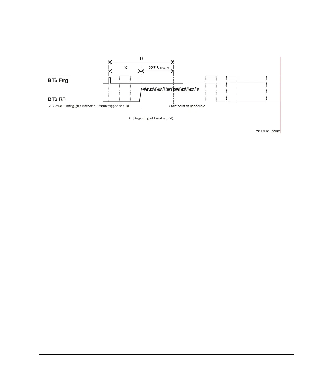
308
Measuring the Initial Delay Value
308
Adjusting the Delay Value
309
Bit Error Rate Tester-Option UN7
312
Block Diagram
312
Clock Gate Function
312
Clock/Gate Delay Function
313
Clock Delay Function
314
Gate Delay Function in the Clock Mode
316
Triggering
316
Data Processing
319
Repeat Measurements
320
Testing Signal Definitions
321
RF Loopback BER-Option 300
323
Synchronization
323
Erased Frame Detection
324
Downlink Errors
324
Frame Structure
324
Verifying BERT Operation
326
Verification Setup
326
CDMA Digital Modulation
331
Cdma2000 Forward Link Modulation for Component Test
332
Activating a Predefined CDMA Forward Link State
332
Creating a User-Defined CDMA Forward Link State
333
Cdma2000 Reverse Link Modulation for Component Test
336
Activating a Predefined Cdma2000 Reverse Link State
336
Creating a User-Defined Cdma2000 Reverse Link State
337
Storing a Component Test Waveform to Memory
340
Recalling a Component Test Waveform
341
Creating a Custom Multicarrier Cdma2000 Waveform
342
Opening the Multicarrier Cdma2000 Setup Table Editor
342
Modifying a Multicarrier Cdma2000 4-Carrier Template
343
Activating a Custom Multicarrier Cdma2000 Setup
344
Cdma2000 Forward Link Modulation for Receiver Test
346
Editing the Base Station Setup
346
Editing Channel Setups
346
Adjusting Code Domain Power
348
Managing Noise
349
Generating the Baseband Signal
350
Configuring the RF Output
351
Cdma2000 Reverse Link Modulation for Receiver Test
352
Editing the Mobile Setup
352
Editing Channel Setups
352
Adjusting Code Domain Power
354
Managing Noise
355
Generating the Baseband Signal
356
Configuring the RF Output
357
Applying a User-Defined FIR Filter to a Cdma2000 Waveform
358
Figure
359
IS-95A Modulation
360
Creating a Predefined CDMA State
360
Creating a User-Defined CDMA State
361
Creating a User-Defined Multicarrier Cdma State
363
Adding a Carrier
363
Applying Changes to an Active CDMA State
363
Selecting a Multicarrier CDMA Setup
363
Generating the Waveform
364
Applying Changes to an Active Multicarrier CDMA State
365
Modifying Carrier Frequency Offset
364
Modifying Carrier Power
364
Press Edit Item > -10 > Db
364
Press Edit Item Khz
364
Configuring the RF Output
365
GPS Modulation
367
Real Time MSGPS
368
Signal Generation Block Diagram
369
Scenario Files
370
RF Power Level Considerations
371
Generating a Real Time MSGPS Signal
373
Configuring the External Reference Clock
374
Real Time GPS
375
Real Time GPS Introduction
376
Setting up the Real Time GPS Signal
381
Configuring the External Reference Clock
382
Testing Receiver Sensitivity
384
Setting up a Gps Bit Error Rate Test
385
Connecting the Test Equipment
386
Setting the Carrier Frequency and Power Level
386
Selecting the BERT Data Pattern and Total Bits
387
Selecting the Data Format
387
Setting up the GPS Receiver
387
Selecting the BERT Trigger
388
Starting BERT Measurements
388
Multitone Waveform Generator
389
Creating a Custom Multitone Waveform
390
Initializing the Multitone Setup Table Editor
390
Configuring Tone Powers and Tone Phases
390
Removing a Tone
390
Generating the Waveform
391
Configuring the RF Output
391
Applying Changes to an Active Multitone Signal
392
Storing a Multitone Waveform
392
Recalling a Multitone Waveform
393
Custom Digital Modulation
395
Using the Arbitrary Waveform Generator
396
Using Predefined Custom TDMA Digital Modulation
396
Creating a Custom TDMA Digital Modulation State
397
Storing a Custom TDMA Digital Modulation State
398
Recalling a Custom TDMA Digital Modulation State
398
Creating a Custom Multicarrier TDMA Digital Modulation State
399
Storing a Custom Multicarrier TDMA Digital Modulation State
401
Applying Changes to an Active Multicarrier TDMA Digital Modulation State
401
Using the Real Time I/Q Baseband Generator
402
Selecting Predefined Custom Modulation Modes
402
Creating User-Defined Custom Modulation
403
Real Time TDMA Formats
405
EDGE Framed Modulation
406
Understanding External Data Connections
406
Activating Framed Data Format
407
Configuring the EDGE Timeslots
407
Configuring GMSK Timeslots
407
Disabling Timeslot Ramping
408
Generating the Baseband Signal
408
Configuring the RF Output
408
Adjusting the Power Level between Timeslots
408
GSM Framed Modulation
410
Activating Framed Data Format
410
Configuring the First Timeslot
410
Configuring the Second Timeslot
410
Configuring the Third Timeslot
410
Disabling Timeslot Ramping
411
Generating the Baseband Signal
411
Configuring the RF Output
411
Adjusting the Power Level between Timeslots
411
Enhanced Observed Time Difference (E-OTD)
412
Overview
412
Basic GSM Frame Structure
412
E-OTD Measurement System Synchronization
418
Sample SCPI Command Scripts
421
DECT Framed Modulation
425
Activating Framed Data Format
425
Configuring the First Timeslot
425
Configuring the Second Timeslot
425
Generating the Baseband Signal
425
Configuring the RF Output
426
PHS Framed Modulation
427
Activating Framed Data Format
427
Configuring the First Timeslot
427
Configuring the Second Timeslot
427
Generating the Baseband Signal
427
Configuring the RF Output
428
PDC Framed Modulation
429
Activating Framed Data Format
429
Configuring the First Timeslot
429
Configuring the Second Timeslot
429
Generating the Baseband Signal
429
Configuring the RF Output
430
NADC Framed Modulation
431
Activating Framed Data Format
431
Configuring the First Timeslot
431
Configuring the Second Timeslot
431
Generating the Baseband Signal
431
Configuring the RF Output
432
TETRA Framed Modulation
433
Activating Framed Data Format
433
Configuring the First Timeslot
433
Configuring the Second Timeslot
433
Generating the Baseband Signal
433
Configuring the RF Output
434
W-CDMA Digital Modulation for Component Test
435
W-CDMA Downlink Modulation
436
Activating a Predefined W-CDMA Downlink State
436
Creating a User-Defined W-Cdma Downlink State
437
Selecting a W-CDMA Downlink Setup
437
Editing Downlink Channel Parameters
438
Clipping the Waveform
440
Storing a W-CDMA Downlink/Uplink State
441
Inserting Additional Channels
440
Applying Channel Modifications to an Active Waveform
441
Configuring the RF Output
441
Recalling a W-CDMA Downlink/Uplink State
442
Creating a User-Defined Multicarrier W-CDMA State
443
Storing a Multicarrier W-CDMA State
446
Recalling a Multicarrier W-CDMA State
447
Generating the Waveform
441
W-CDMA Uplink Modulation
448
Creating a Predefined W-CDMA Uplink State
448
Creating a User-Defined W-Cdma Uplink State
449
Selecting a W-CDMA Uplink Setup
449
Editing Uplink Channel Parameters
450
Inserting Additional Channels and Modifying I/Q Settings
450
Clipping the Waveform
451
Generating the Waveform
451
Applying Channel Modifications to an Active Waveform
452
Configuring the RF Output
452
W-CDMA Concepts
453
Understanding TPC Values
455
Understanding TFCI, TPC, and Pilot Power Offsets
456
Calculating Downlink Scramble Codes
458
W-CDMA Frame Structures
462
Downlink PICH Frame Structure
462
Downlink PCCPCH + SCH Frame Structure
463
Downlink DPCCH/DPDCH Frame Structure
464
Uplink DPCCH/DPDCH Frame Structure
466
W-CDMA Uplink Digital Modulation for Receiver Test
469
Equipment Setup
471
ESG and Agilent E4440A PSA Spectrum Analyzer Setup
471
ESG and Base Transceiver Station (BTS) Setup
471
Understanding the PRACH
473
Overview
473
Access Slots
473
Preamble
474
Message Part
475
Power Control
477
Power Control Modes
483
Generating a Single PRACH Signal
486
Configuring the RF Output
486
Selecting the PRACH and Single PRACH Modes
486
Selecting a Rear Panel Output Trigger
486
Generating the Baseband Signal
487
Setting up the E4440A PSA for the PRACH Signal
487
Modifying the PRACH Physical and Transport Layers
488
Viewing the Modified PRACH Signal
492
Generating the AICH for the PRACH Message Transmission
492
Viewing the PRACH Message Using an AICH Trigger
495
Using the AICH Feature with a Base Transceiver Station
496
Multiple PRACH Overview
498
Understanding the 80 Ms Transmission/Time Period
498
Understanding the Power Offset between the Carrier and the Multiple PRACH
501
Setting up a Multiple PRACH Signal
503
Configuring the RF Output
503
Selecting the PRACH and Multiple PRACH Modes
504
Selecting the Rear Panel Output Trigger
504
Generating the Baseband Signal
505
Configuring the PRACH Code Setup
505
Configuring the PRACH Power Setup
511
Configuring the PRACH Timing Setup
514
Viewing a Multiple PRACH Signal
519
Connecting the ESG to a Base Station
520
Overload Testing with Multiple Prachs-Multiple Esgs
521
Connecting the ESG to the Base Transceiver Station
523
Configuring the Esgs
524
Setting up the LF Output as the PRACH Start Trigger Signal
527
Dpch
528
Generating a DPCCH/DPDCH with a Reference Measurement Channel
528
Configuring the E4440A PSA for Viewing the DPCCH/DPDCH Output
529
Modifying the DPCCH/DPDCH Physical and Transport Layers
530
Configuring the E4440A PSA for Viewing Additive Noise
534
Adding Noise
534
Using the Transmit Power Control
537
Compressed Mode Single Transmission Gap Pattern Sequence (TGPS) Overview
541
Setting up Compressed Mode for a Single TGPS Transmission
543
Equipment Setup
543
Configuring the RF Output
543
Accessing the W-CDMA Modulation Format and Selecting Uplink
544
Setting up the W-CDMA Signal Parameters
544
Generating the Baseband Signal
545
Configuring Compressed Mode
545
Viewing and Adjusting the Compressed Mode Signal
549
Compressed Mode Multiple Transmission Gap Pattern Sequence (TGPS) Overview
552
Understanding Multiple TGPS Compressed Frame Alignment
552
Setting up Compressed Mode for a Multiple TGPS Transmission
555
Equipment Setup
555
Configuring the RF Output
555
Accessing the W-CDMA Modulation Format and Selecting Uplink
556
Setting up the W-CDMA Signal Parameters
556
Selecting the Rear Panel Output Trigger
557
Generating the Baseband Signal
557
Configuring TGPSI 1
558
Configuring TGPSI 2
561
Viewing the Multiple TGPSI Signal
564
Configuring the UE Setup
566
Locating Rear Panel Input Signal Connectors
567
Configuring Rear Panel Output Signals
569
Accessing the Output Trigger Signal Menu
569
Selecting an Output Signal
569
Deselecting an Output Signal
571
Adjusting Code Domain Power
572
Scaling to 0 Db
572
Setting Equal Channel Powers
573
W-CDMA Uplink Concepts
574
Data Channel Air Interface Block Diagram
574
Reference Measurement Channels (RMC)
574
Transition between Normal Frame and Compressed Frame
575
Settling Time During User Event for DPCH Compressed Mode
576
Connecting the ESG to a W-CDMA Base Station
576
Connector Assignments for W-CDMA Uplink
577
Signal Descriptions for W-CDMA Uplink
581
Synchronization Diagrams
586
Frame Sync Trigger Status Indicator
591
Prach
594
W-CDMA AWGN Measurements and Bandwidths
595
DPCH Transmit Power Control by an External Signal
597
DPCCH/DPDCH Frame Structure
599
W-Cdma Downlink Digital Modulation for Receiver Test
601
Using W-CDMA Downlink
602
Configuring the Base Station Setup
602
Configuring the Physical Layer
603
Configuring the Transport Layer
604
Adjusting Code Domain Power
605
Managing Noise
607
Generating the Baseband Signal
608
Applying New Settings
608
Configuring the RF Output
609
Transmit Diversity Overview
610
Configuring for Transmit Diversity and BERT
613
Equipment Set up
613
Configuring the RF Output for both Esgs
614
Accessing the W-CDMA Modulation Format and Selecting Downlink
615
Setting up Antenna One (ESG One)
615
Setting up Antenna Two (ESG Two)
619
Generating the Baseband Signals and Synchronizing the ESG Transmissions
621
Configuring the UE
621
Making the BERT Measurement
622
Out-Of-Synchronization Testing Overview
624
Configuring for Out-Of-Synchronization Testing
625
Equipment Set up
625
Setting the RF Output
626
Accessing the W-CDMA Modulation Format and Selecting Downlink
627
Setting up the W-CDMA Signal Parameters
627
Selecting the Input DTX Gating Signal Trigger Polarity
628
Generating the Baseband Signal and Activating the Out-Of-Synchronization Test Feature
629
Configuring the UE
629
Setting up the Spectrum Analyzer for Detecting the UE DTX
629
Configuring the DPCH DTX Gating Trigger Signal
630
Compressed Mode Overview
631
Setting up for a Compressed Mode Signal
634
Equipment Setup
634
Setting the RF Output
636
Accessing the W-CDMA Modulation Format and Selecting Downlink
637
Setting up the W-CDMA Signal Parameters
637
Generating the Baseband Signal
638
Configuring Compressed Mode
638
Making Compressed Mode Signal Measurements
643
Measuring the DPCH Symbol Power
643
Making the BERT Measurement
647
Locating Rear Panel Input Signal Connectors
649
Configuring Rear Panel Output Signals
651
Accessing the Rear Panel Output Signal Menu
651
Selecting an Output Signal
651
Deselecting an Output Signal
652
Rear Panel Output Signal Descriptions
653
W-CDMA Downlink Concepts
656
DPCH Coding Block Diagram
656
Reference Measurement Channels
656
Scramble Codes
658
W-CDMA AWGN Measurements and Bandwidths
659
Special Power Control Considerations When Using Compressed Mode
662
W-CDMA Frame Structures
663
Downlink PICH Frame Structure
663
Downlink PCCPCH + SCH Frame Structure
664
Downlink DPCCH/DPDCH Frame Structure
665
Troubleshooting
667
If You Encounter a Problem
668
Basic Signal Generator Operations
669
Cannot Turn off Help Mode
669
No RF Output
669
Signal Loss While Working with Mixers
670
Signal Loss While Working with Spectrum Analyzers
671
RF Output Power too Low
673
No Modulation at the RF Output
674
Sweep Appears to be Stalled
674
Cannot Turn off Sweep Mode
674
Incorrect List Sweep Dwell Time
675
List Sweep Information Is Missing from a Recalled Register
675
Data Storage
676
Signal Generator Lock-Up
677
Fail-Safe Recovery Sequence
677
Error Messages
679
Error Message File
679
Error Message Format
680
Error Message Types
681
Upgrading Firmware
682
Returning a Signal Generator to Agilent Technologies
683
Contacting Agilent Sales and Service Offices
684
Other manuals for Agilent Technologies E4428C
Programming Guide
366 pages
Configuration Guide
12 pages
5
Based on 1 rating
Ask a question
Give review
Questions and Answers:
Need help?
Do you have a question about the Agilent Technologies E4428C and is the answer not in the manual?
Ask a question
Agilent Technologies E4428C Specifications
General
Brand
Agilent Technologies
Model
E4428C
Category
Inverter
Language
English
Related product manuals
Agilent Technologies E8257D
366 pages
Agilent Technologies E8267D
366 pages
Agilent Technologies E8257D PSG
318 pages
Agilent Technologies 33220A
363 pages
Agilent Technologies 33120A
312 pages
Agilent Technologies 33250A
336 pages
Agilent Technologies 83620B
496 pages
Agilent 33500 Series
429 pages