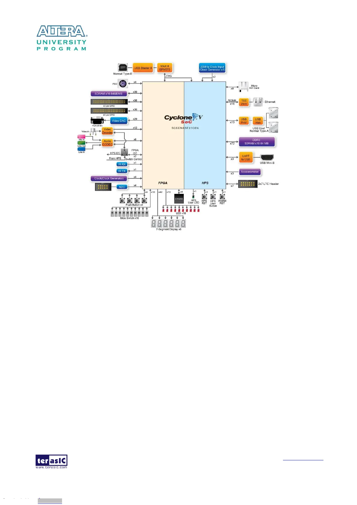
Figure 2-3 Block diagram of DE1-SoC
Detailed information about Figure 2-3 are listed below.
Cyclone V SoC 5CSEMA5F31 Device
Dual-core ARM Cortex-A9 (HPS)
85K programmable logic elements
4,450 Kbits embedded memory
6 fractional PLLs
2 hard memory controllers
C
C
o
o
n
n
f
f
i
i
g
g
u
u
r
r
a
a
t
t
i
i
o
o
n
n
a
a
n
n
d
d
D
D
e
e
b
b
u
u
g
g
Quad serial configuration device – EPCQ256 on FPGA
Onboard USB-Blaster II (normal type B USB connector)
Downloaded from Arrow.com.Downloaded from Arrow.com.Downloaded from Arrow.com.Downloaded from Arrow.com.Downloaded from Arrow.com.Downloaded from Arrow.com.Downloaded from Arrow.com.Downloaded from Arrow.com.Downloaded from Arrow.com.Downloaded from Arrow.com.