9-1
Chapter 9. LIST OF COMMUNICATION DATA
List of communication data
The following shows the meanings of the symbols stated in the “RAM/EEPROM Read/Write” columns:
No symbol: Possible.
*: Possible according to the conditions.
∆: Possible, but data is invalid.
X: Impossible.
Note: When reading the EEPROM address, data in the RAM is read in the same manner as reading of the
RAM address.
Decimal point information:
—: No decimal point
1 to 3: Decimal point position (The communication data becomes that the original value is
multiplied by 10, 100, or 1000.)
P: Follows the PV input range.
S: Follows various conditions.
RS/WS commands of CPL communication Decimal data address with “W” attached next to it is
used.
RD/WD/RU/WU commands of CPL communication: Hexadecimal data address is used.
Commands of Modbus communication: Hexadecimal data address is used.
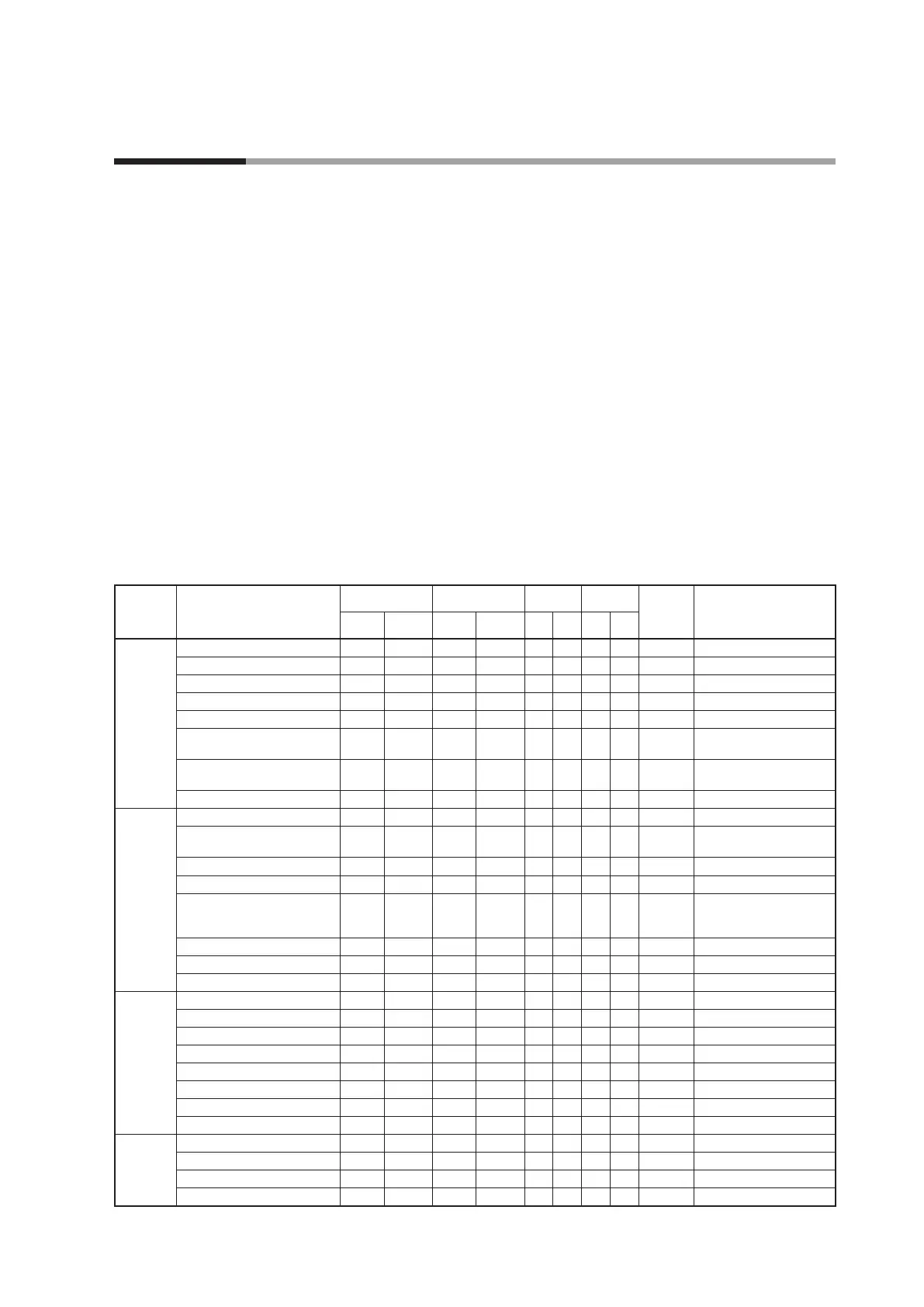
Bank
Item name
RAM address EEPROM address RAM EEPROM
Decimal
point
information
Notes
Decimal
Hexadecimal
Decimal
Hexadecimal
Read Write Read Write
Instrument
information
ROM ID
273 0111 16657 4111 X X —
"2" when using SDC35/36.
ROM Version 1
274 0112 16658 4112 X X 2
ROM Version 2
275 0113 16659 4113 X X 2
LOADER Information
276 0114 16660 4114 X X —
EST Information
277 0115 16661 4115 X X —
Manufacturing date code (year)
278 0116 16662 4116 X X —
Year - 2000 Example:
Year of 2003 is expressed as "3"
Manufacturing date code (month,
day)
279 0117 16663 4117 X X 2
Month + (Day ÷ 100) Example:
Dec. 1st is expressed as "12.01".
Serial No.
280 0118 16664 4118 X X —
Lock
Key lock
5001 1389 21385 5389 —
Communication lock
5002 138A 21386 538A * X * X —
When the communication lock
exists, the error response is sent.
Loader lock
5003 138B 21387 538B X X —
Password display
5004 138C 21388 538C X —
Password 1A
— — — — X X X X —
Communication and loader
cannot read and write the
password.
Password 2A
— — — — X X X X —
Same as above.
Password 1B
— — — — X X X X —
Same as above.
Password 2B
— — — — X X X X —
Same as above.
User Function
User Function 1
5101 13ED 21485 53ED —
User Function 2
5102 13EE 21486 53EE —
User Function 3
5103 13EF 21487 53EF —
User Function 4
5104 13F0 21488 53F0 —
User Function 5
5105 13F1 21489 53F1 —
User Function 6
5106 13F2 21490 53F2 —
User Function 7
5107 13F3 21491 53F3 —
User Function 8
5108 13F4 21492 53F4 —
Setup
PV input range type
5201 1451 21585 5451 —
Temperature unit
5202 1452 21586 5452 * * —
Cold junction compensation (T/C)
5203 1453 21587 5453 * * —
Decimal point position
5204 1454 21588 5454 * * —
(Continue on next page.)
 Loading...