Camera Interface
Basler A500k Series 2-7
PRELIMINARY
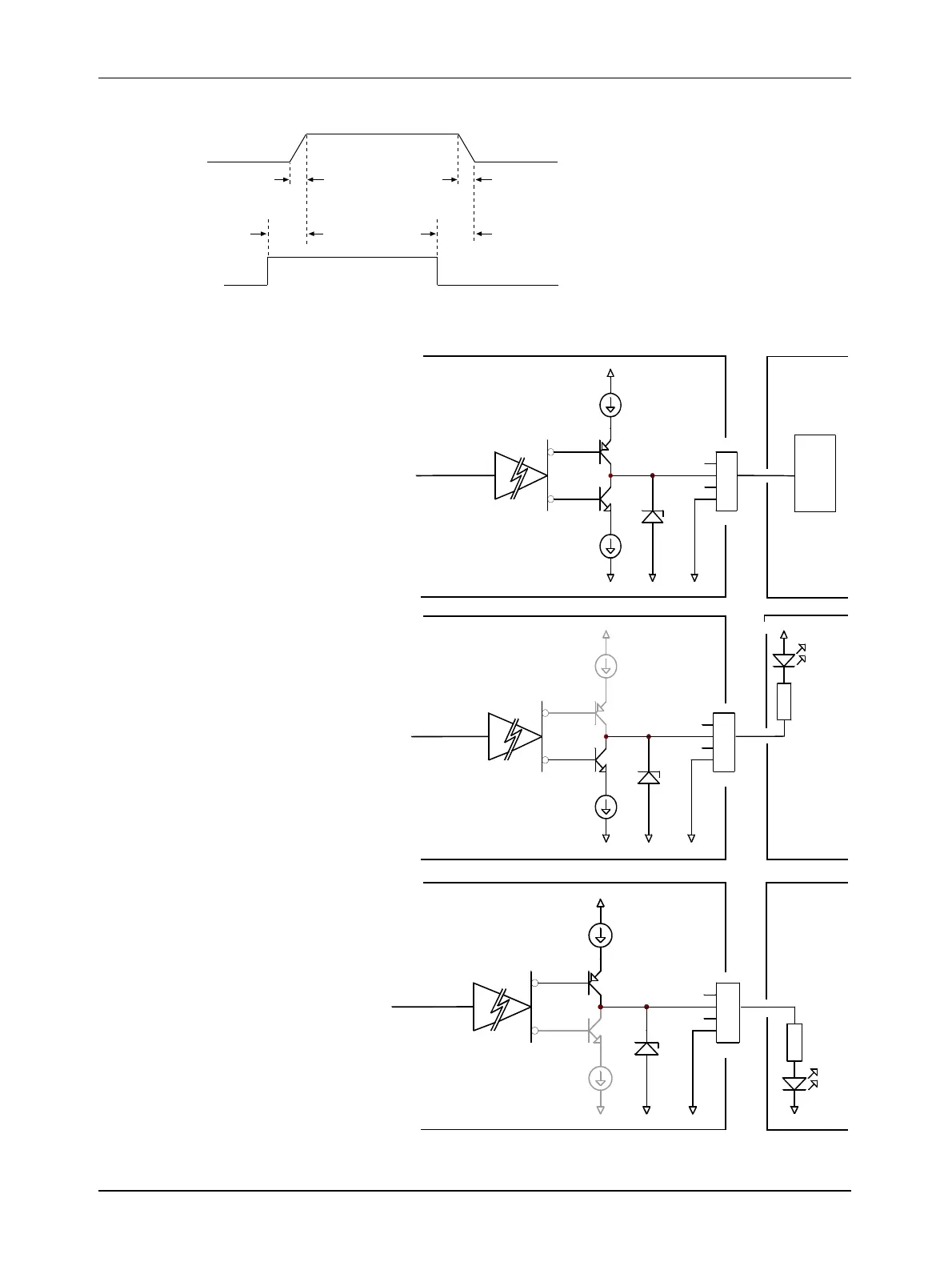
Figure 2-3: FlashOut Signal Timing
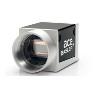
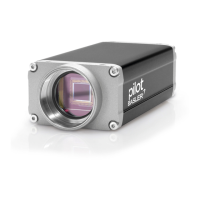
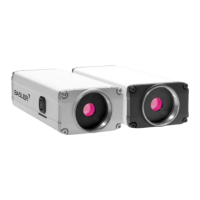
Figure 2-4: Flash Trigger Output Schematics
Flash
Out
ExFlash
or
Internal
Effective
Exposure
max = 0.3 µs max = 0.3 µs
max
= 1.3 µs (A501k)
= 1 µs (A504k)
max = 1.3 µs (A501k)
= 1 µs (A504k)
ca. 50 mA
ca. 50 mA
5.6V
1
2
3
4
Connector
HR10-7R-4SA
ISO +5 V
ISOGND ISOGND ISOGND
Flash Signal
TTL /
CMOS
Logic
Device
ca. 50 mA
ca. 50 mA
5.6 V
1
2
3
4
Connector
HR10-7R-4SA
ISO +5V
ISOGND ISOGND ISOGND
Flash Signal
typically +5 V to 24 V
ca. 50 mA
ca. 50 mA
5.6 V
1
2
3
4
Connector
HR10-7R-4SA
ISO +5 V
ISOGND ISOGND ISOGND
Flash Signal
GND
TTL Active High (default)
A TTL Active High output signal is
typically used together with a TTL /
CMOS Logic Device.
The TTL Active High output signal
has the following characteristics:
• High output min. 4.5 V at 10 mA
output load, shortcut current
50 mA (+40%/- 20%)
• Low output max. 0.5 V at -10 mA
output load, shortcut current -
50 mA (+40%/- 20%)
Low Side Switch
(Open Collector)
When you select this output signal
variant, the upper transistor is deac-
tivated, which is shown by grayed
lines in the schematic.
The schematic shows a sample cir-
cuit for your flash device.
Calculate your devices so that the
maximum output current is 50 mA.
High Side Switch
When you select this output signal
variant, the lower transistor is deac-
tivated, which is shown by grayed
lines in the schematic.
The schematic shows a sample
circuit for your flash device.
Calculate your devices so that the
maximum output current is 50 mA.
camera
camera
camera
flash
device
flash
device
flash
device