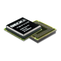
IPC@CHIP SC123/SC143
Hardware Manual V1.06 [18.02.2010]
©2000-2008 BECK IPC GmbH Page 6
List of Tables
Table 4-1: Pin Description of System Interface ............................................................................................................. 12
Table 4-2: Pin Description of Chip Selects .................................................................................................................... 13
Table 4-3: Pin Description of DMA Request Pins .......................................................................................................... 14
Table 4-4: Pin Description of Interrupts ......................................................................................................................... 14
Table 4-5: Pin Description of UART0............................................................................................................................. 14
Table 4-6: Pin Description of UART1............................................................................................................................. 15
Table 4-7: Pin Description of UART2............................................................................................................................. 15
Table 4-8: Pin Description of I²C Bus ............................................................................................................................ 16
Table 4-9: Pin Description of Pure PIO pins .................................................................................................................. 16
Table 4-10: Pin Description of SPI Bus / UART3 ........................................................................................................... 17
Table 4-11: Pin Description of Timers ........................................................................................................................... 17
Table 4-12: Pin Description of CAN Bus ........................................................................................................................ 18
Table 4-13: Pin Description of USB ............................................................................................................................... 18
Table 4-14: Pin Description of JTAG ............................................................................................................................. 18
Table 4-15: Pin Description of internal PHY .................................................................................................................. 19
Table 4-16: Pin Description of MII ................................................................................................................................. 19
Table 4-17: Pin Description of PHY Power Pins ............................................................................................................ 20
Table 4-18: Pin Description of Power Pins .................................................................................................................... 20
Table 4-19: List of PIO sharing designations. ................................................................................................................ 21
Table 6-1: General Purpose Registers .......................................................................................................................... 24
Table 6-2: Segment, Status and Control Registers ....................................................................................................... 24
Table 6-3: Segment Register Selection Rules ............................................................................................................... 25
Table 6-4:Context between SDO and SDI to MOSI and MISO in different modes ........................................................ 34
Table 6-5: Provided CAN baud rates ............................................................................................................................. 36
Table 6-6: Truth Table of FLSSEL and UCSOUT# and external memory ..................................................................... 40
Table 8-1: Absolute Maximum Ratings .......................................................................................................................... 44
Table 8-2: Recommended Operating Ranges ............................................................................................................... 44
Table 8-3: Supply Current ............................................................................................................................................. 44
Table 8-4: Inputs ........................................................................................................................................................... 45
Table 8-5: Outputs ......................................................................................................................................................... 45
Table 8-6: PIOs ............................................................................................................................................................. 45
Table 8-7: 3. I/O Characteristics Xin/Xout Pins ............................................................................................................. 45
Table 8-8: PHY Receiver Input Characteristics ............................................................................................................. 46
Table 8-9: 100Base-TX Transceiver Characteristics ..................................................................................................... 46
Table 8-10: AC Characteristics ...................................................................................................................................... 47
Table 10-1: Package Dimensions .................................................................................................................................. 52
Table 13-1: Typical Reflow Profile Conditions ............................................................................................................... 60