The GPIO_DOUT register contains the following sub-fields:
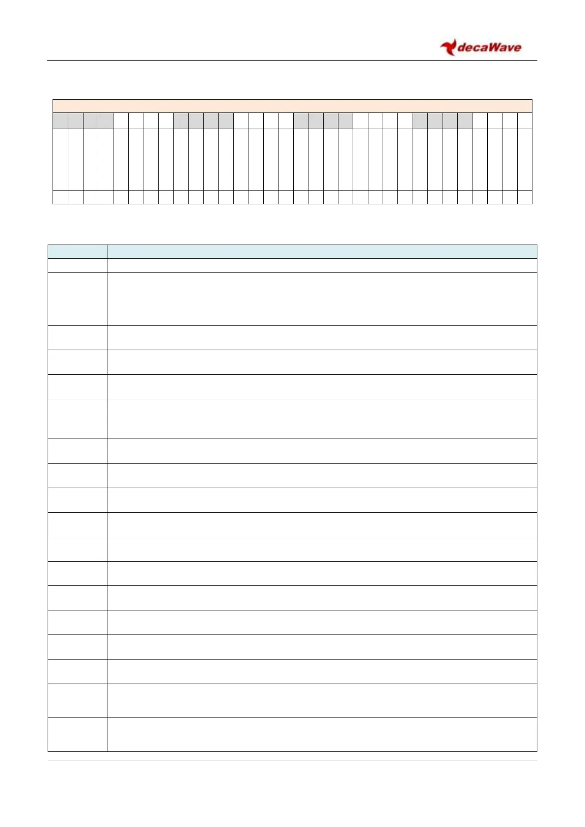
REG:26:0C – GPIO_DOUT – GPIO Data Output register
The fields of the GPIO_DOUT register identified above are individually described below:
Description of fields within Sub-Register 0x26:0C – GPIO_DOUT
Bits marked ‘-’ are reserved and should be written as zero.
Output state setting for the GPIO0 output. Reading this bit shows the current setting for
GPIO0. Value 1 = logic 1 voltage high output and, value 0 = logic 1 voltage low output. When
writing (either 1 or 0) to this GOP0 bit, its value is only changed if the GOM0 mask bit has a
value of 1 in that write operation.
Output state setting for GPIO1. (See GOP0).
Output state setting for GPIO2. (See GOP0).
Output state setting for GPIO3. (See GOP0).
Mask for setting GPIO0 output state. When writing to GOP0 to select state of the GPIO0
output, the value of GOP0 is only changed if this GOM0 mask bit has a value of 1 for the write
operation. GOM0 will always read as 0.
Mask for setting GPIO1 output state. (See GOM0).
Mask for setting GPIO2 output state. (See GOM0).
Mask for setting GPIO3 output state. (See GOM0).
Output state setting for GPIO4. (See GOP0).
Output state setting for GPIO5. (See GOP0).
Output state setting for GPIO6. (See GOP0).
Output state setting for GPIO7. (See GOP0).
Mask for setting the GPIO4 output state. (See GOM0).
Mask for setting the GPIO5 output state. (See GOM0).
Mask for setting the GPIO6 output state. (See GOM0).
Mask for setting the GPIO7 output state. (See GOM0).
Output state setting for GPIO8. (See GOP0).