Circuit Descriptions
3.3 Detailed Circuit Descriptions
3
3-9
3.3 Detailed Circuit Descriptions
3.3.1 Power Circuit
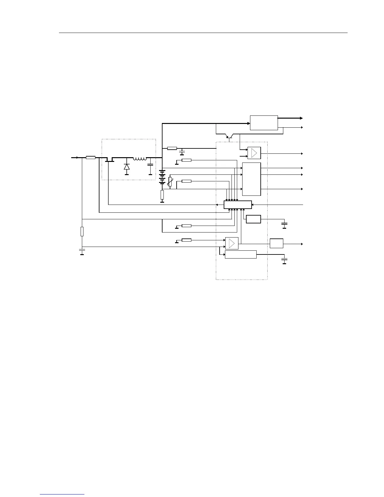
The description below refers to circuit diagram Figure 9-5.
Power Sources , Operating Modes
Figure 3-3 shows a simplified diagram of the power supply and battery charger circuit.
V566
R516
R514
R502
R512
R513
P7VCHA
60
BATCU
V569
R506
R507
V565
CHARGER/CONVERTER
SUPPLY
linear regulator
18
VGARDRIVE
Figure 3-3. Power Supply Block Diagram
As described in Section 3.2.5, the test tool operating mode depends on the connected
power source.
The voltage VBAT is supplied either by the power adapter via V506/L501, or by the
battery pack. It powers a part of the P-ASIC via R503 to pin 60 (VBATSUP). If the test
tool is off, the Fly Back Converter is off, and VBAT powers the D-ASIC via transistor
V569 (+3V3GAR). This +3V3GAR voltage is controlled and sensed by the P-ASIC. If
it is NOT OK (<3.05V), the output VGARVAL (pin 64) is low. The VGARVAL line is
connected to the D-ASIC, and if the line is low, the D-ASIC is inactive: the test tool is in
the Idle mode. A low VGARVAL line operates as a reset for the D-ASIC.
If VGARVAL is high (+3V3GAR > 3.05V), the D-ASIC becomes active, and the Off
mode is entered. The D-ASIC monitors the P-ASIC output pin 12 MAINVAL, and the
test tool ON/OFF status. By pressing the ON/OFF key, a bit in the D-ASIC indicating
the test tool ON/OFF status is toggled. If no correct power adapter voltage is supplied
(MAINVAL is low), and the test tool is not turned on, the Off mode will be maintained.
If a correct power adapter voltage is supplied (MAINVAL high), or if the test tool is
turned on, the mask software starts up. The mask software checks if valid instrument
software is present. If not, e.g. no instrument firmware is loaded, the mask software will

 Loading...