Circuit Descriptions
3.3 Detailed Circuit Descriptions
3
3-15
3.3.2 Input 1 - Input 2 Measurement Circuits
The description below refers to circuit diagrams Figure 9-1 and Figure 9-2.
The Input 1 and Input 2 circuits are partly identical. Both circuits condition input
voltages. See section 3.2.1 for a description of the differences between Input 1 and 2.
The Input 1/2 circuitry is built-up around a C-ASIC OQ0258. The C-ASIC is placed
directly behind the input connector and transforms the input signal to levels that are
suitable for the ADC and trigger circuits.
The C-ASIC
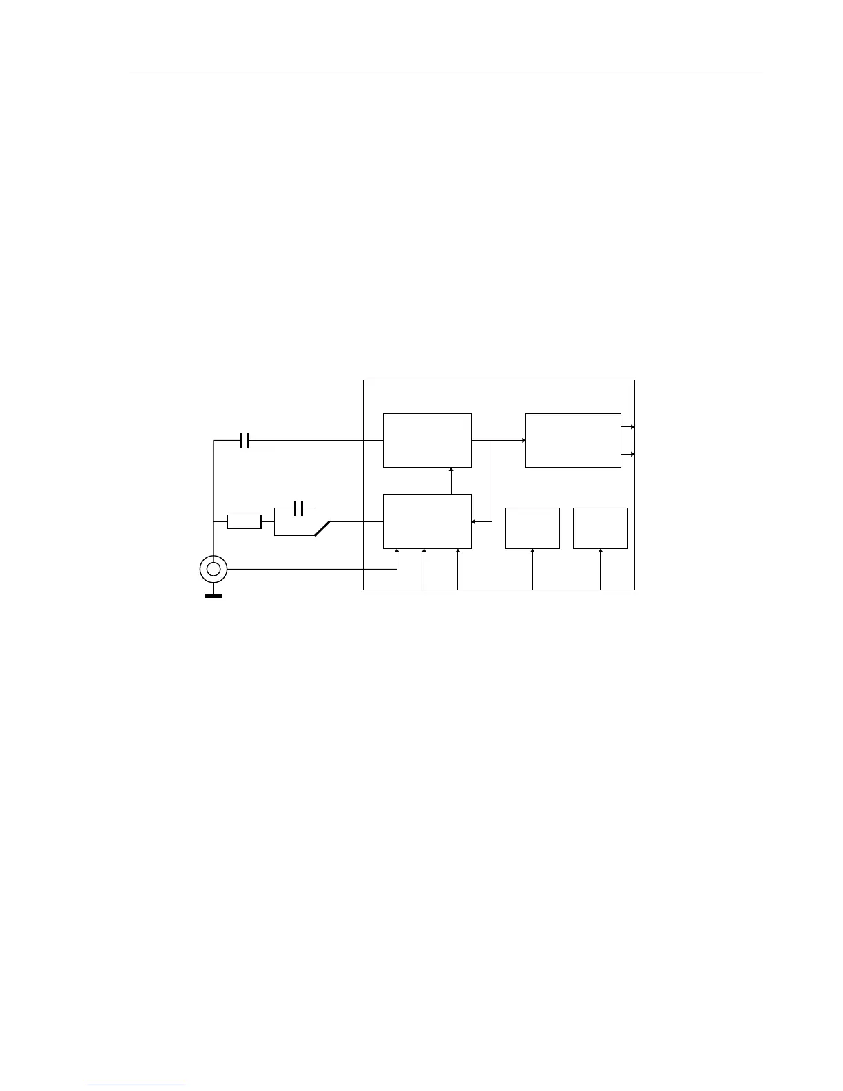
Figure 3-8 shows the simplified C-ASIC block diagram. The C-ASIC consists of
separate paths for HF and LF signals, an output stage that delivers signals to the trigger
and ADC circuits and a control block that allows software control of all modes and
adjustments. The transition frequency from the LF-path to the HF-path is approximately
20 kHz, but there is a large overlap.
HF-PATH
LF-PATH
OUTPUT
STAGE
ADC
TRIGGER
CONTROL SUPPLY
GROUND
LF IN
HF IN
AC
DC
C
R
INPUT
CAL POS BUS SUPPLY
CHANNEL ASIC OQ 0258
PROTECT
Figure 3-8. C-ASIC Block Diagram
LF input
The LF-input (pin 42) is connected to a LF decade attenuator in voltage mode, or to a
high impedance buffer for resistance and capacitance measurements. The LF decade
attenuator consists of an amplifier with switchable external feedback resistors R131 to
R136. Depending on the selected range the LF attenuation factor which will be set to 1-
10-100-1000-10,000. The C-ASIC includes a LF pre-amplifier with switchable gain
factors for the 1-2-5 steps.
HF input (not used for Input 2)
The HF component of the input signal is supplied to four external HF capacitive
attenuators via C104. Depending on the required range, the C-ASIC selects and buffers
one of the attenuator outputs :1 (HF0), :10 (HF1), :100 (HF2), or :1000 (HF3). By
attenuating the HF3 input internally by a factor 10, the C-ASIC can also create a :10000
attenuation factor. Inputs of not selected input buffers are internally shorted. To control
the DC bias of the buffers inputs, their output voltage is fed back via an internal feed
back resistor and external resistors R115, R111/R120, R112, R113, and-R114. The
internal feed back resistor and filter R110/C105 will eliminate HF feed back, to obtain a

 Loading...