43B
Service Manual
3-14
The D-ASIC controls the transmit data line TXD. If the line is low, diode H521 will
emit light.
The supply voltage for the optical interface receive circuit (RXDA), is the +3V3SADC
voltage. The +3V3SADC voltage is present if the test tool is turned on, or if the Power
Adapter is connected (or both). So if the Power Adapter is present, serial
communication is always possible, even when the test tool is off.
Backlight Converter
The LCD back light is provided by a ∅2.4 mm fluorescent lamp in LCD unit. The back
light converter generates the 300-400 Vpp ! supply voltage. The circuit consist of:
• A pulse width modulated (PWM) buck regulator to generate a variable, regulated
voltage (V600, V602, L600, C602).
• A zero voltage switched (ZVS) resonant push-pull converter to transform the
variable, regulated voltage into a high voltage AC output (V601, T600).
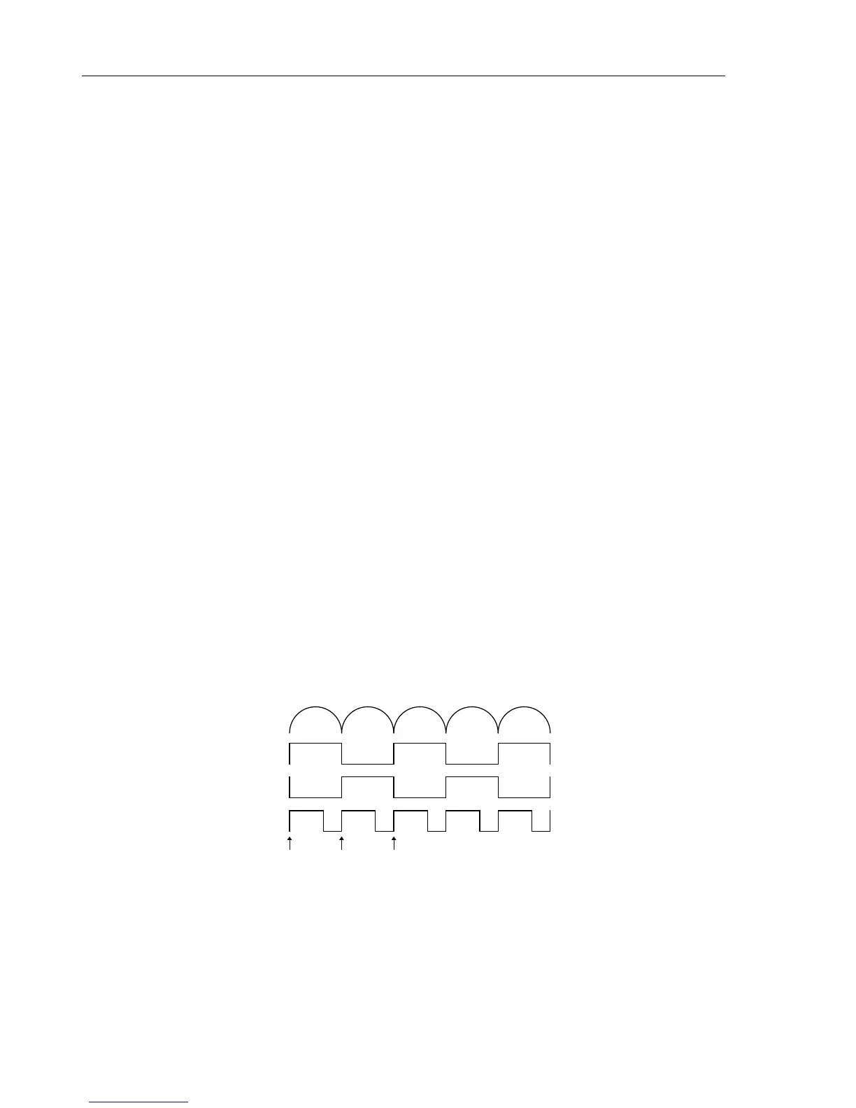
The PWM buck regulator consists of FET V600, V602, L600, C602, and a control circuit
in N600. FET V600 is turned on and off by a square wave voltage on the COUT output
of N600 pin 14). By changing the duty cycle of this signal, the output on C602 provides
a variable, regulated voltage. The turn on edge of the COUT signal is synchronized with
each zero detect.
Outputs AOUT and BOUT of N600 provide complementary drive signals for the push-
pull FETs V601a/b (dual FET). If V601a conducts, the circuit consisting of the primary
winding of transformer T600 and C608, will start oscillating at its resonance frequency.
After half a cycle, a zero voltage is detected on pin 9 (ZD) of N600, V601a will be
turned off, and V601b is turned on. This process goes on each time a zero is detected.
The secondary current is sensed by R600/R604, and fed back to N600 pin 7 and pin 4 for
regulation of the PWM buck regulator output voltage. The BACKBRIG signal supplied
by the D-ASIC provides a pulse width modulated (variable duty cycle) square wave. By
changing the duty cycle of this signal, the average on-resistance of V604 can be changed.
This will change the secondary current, and thus the back light intensity. The voltage on
the “cold” side of the lamp is limited by V605 and V603. This limits the emission of
electrical interference.
R605 and R606 provide a more reliable start-up of the backlight (PCB version 3 up
only).
Voltage at T600 pin 4
Voltage AOUT
Voltage BOUT
Voltage COUT
zero
detect
zero
detect
Figure 3-7. Back Light Converter Voltages

 Loading...