43
V554
72
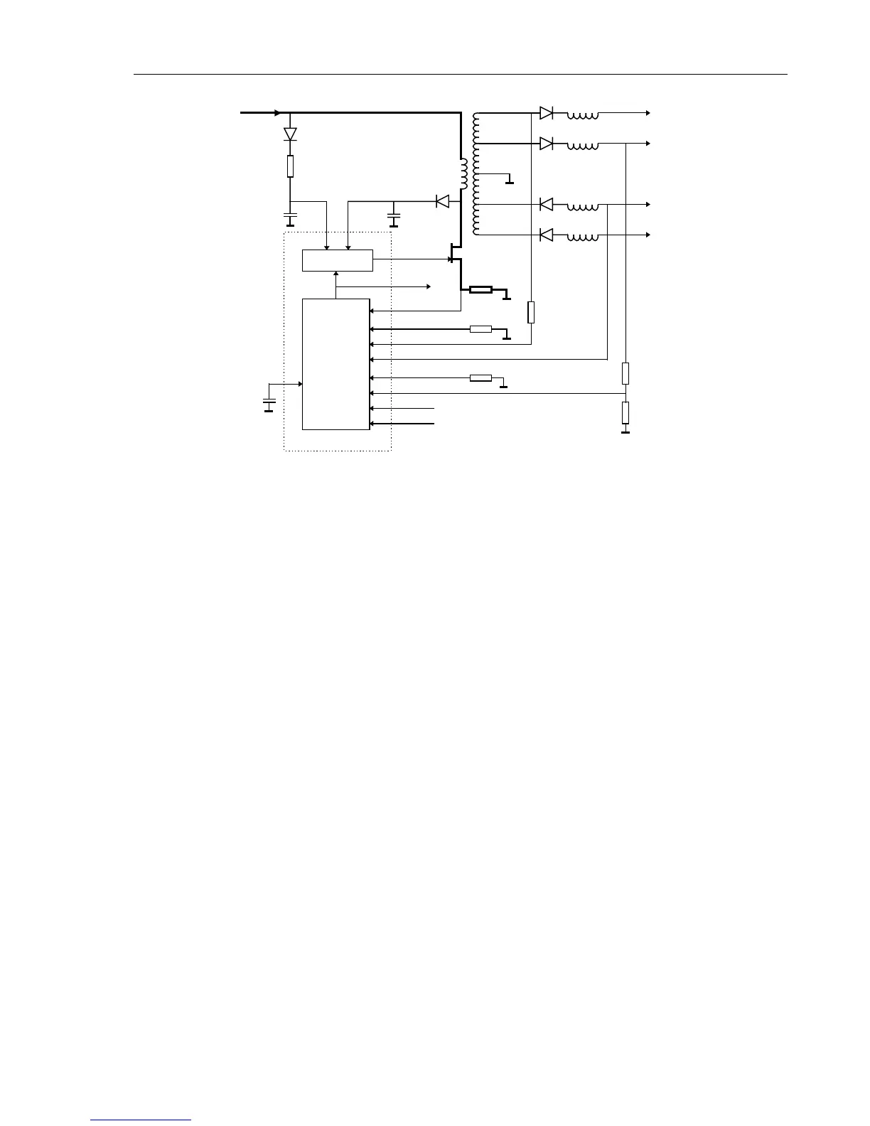
Figure 3-6. Fly-Back Converter Block Diagram
Slow ADC
The Slow ADC enables the D-ASIC to measure the following signals:
BATCUR, BATVOLT, BATTEMP, BATIDENT (Battery current, - voltage, -
temperature, - type ), DACTEST-A, DACTEST-B, and DACTEST-T (test output of the
C-ASIC’s and the T-ASIC).
De-multiplexer D531 supplies one of these signals to its output, and to the input of
comparator N531 TP536). The D-ASIC supplies the selection control signals
SELMUX0-2. The Slow ADC works according to the successive approximation
principle. The D-ASIC changes the SADCLEV signal level, and thus the voltage level
on pin 3 of the comparator step wise, by changing the duty cycle of the PWM signal
SADCLEVD. The comparator output SLOWADC is monitored by the D-ASIC, who
knows now if the previous input voltage step caused the comparator output to switch. By
increasing the voltage steps, the voltage level can be approximated within the smallest
possible step of the SADCLEV voltage. From its set SADCLEVD duty cycle, the D-
ASIC knows voltage level of the selected input.
RS232
The optical interface enables serial communication (RS232) between the test tool and a
PC or printer.
The received data line RXDA (P-ASIC pin 75) is connected to ground via a 20 kΩ
resistor in the P-ASIC.
If no light is received by the light sensitive diode H522, the RXDA line is +200 mV,
which corresponds to a “1” (+3V) on the RXD (P-ASIC output pin 76) line.
If light is received, the light sensitive diode will conduct, and the RXDA line goes low
(0...-0.6V), which corresponds to a “0” on the RXD line.
The level on the RXDA line is compared by a comparator in the P-ASIC to a 100 mV
level. The comparator output is the RXD line, which is supplied to the D-ASIC for
communication, and for external triggering.

 Loading...