Circuit Descriptions
3.3 Detailed Circuit Descriptions
3
3-11
charge current is applied for 48 hours maximum. If the battery temperature becomes
higher than 50°C, the charge current is set to zero.
Battery temperature monitoring
The P-ASIC supplies a current to a NTC resistor in the battery pack (TEMP pin 5). It
conditions the voltage on pin 5 and supplies it to output pin 79 BATTEMP. The D-ASIC
measures this voltage via the slow ADC. It uses the BATTEMP voltage to decide if fast
charge is allowed (10-45°C), or no charge is allowed at all (<10°C, >50°C).
Additionally the temperature is monitored by the P-ASIC. The P-ASIC supplies a
current to reference resistor R512 (TEMPHI pin 4), and compares the resulting TEMPHI
voltage to the voltage on pin 5 (TEMP). If the battery temperature is too high, the
P-ASIC Control circuit sets the charge current to zero, in case the D-ASIC fails to do
this.
If the battery temperature monitoring system fails, a bimetal switch in the battery pack
interrupts the battery current if the temperature becomes higher then 70 °C.
Maximum VBAT
The P-ASIC supplies a current to reference resistor R513 (VBATHIGH pin 7). It
compares the voltage on R513 to the battery voltage VBAT on pin 3 (after being
attenuated in the P-ASIC). The P-ASIC limits the voltage VBAT to 7.4V via its internal
Control circuit. This happens if no battery or a defective battery (open) is present.
Charger/Converter input current
This input current is sensed by R501. The P-ASIC supplies a reference current to R514.
The P-ASIC compares the voltage drop on R501 (P-ASIC pin 14 and 15) to the voltage
on R514 (IMAXCHA pin 6). It limits the input current (e.g. when loading C503/C555
just after connecting the power adapter) via its internal Control circuit.
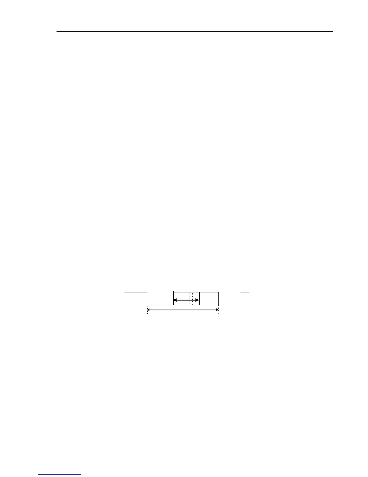
CHAGATE control signal
To make the FET conductive its Vgs (gate-source voltage) must be negative. For that
purpose, the CHAGATE voltage must be negative with respect to VCHDRIVE. The
P-ASIC voltage VCHDRIVE also limits the swing of the CHAGATE signal to 13V.
VCHDRIVE
VCHDRIVE -13V
10
µ
s
V506 “OFF”
V506 “ON”
Figure 3-4. CHAGATE Control Voltage
+3V3GAR Voltage
When the test tool is not turned on, the Fly Back Converter does not run. In this
situation, the +3V3GAR voltage for the D-ASIC, the FlashROM, and the RAM is
supplied via transistor V569. The voltage is controlled by the VGARDRV signal
supplied by the P-ASIC (pin 69). The current sense voltage across R580 is supplied to
pin 70 (VGARCURR). The voltage +3V3GAR is sensed on pin 66 for regulation. The
internal regulator in the P-ASIC regulates the +3V3GAR voltage, and limits the current.

 Loading...