Circuit Descriptions
3.3 Detailed Circuit Descriptions
3
3-17
DACTEST output pin 24
As described above, the DACTEST output is used for signaling a ground protect error. It
can also be used for testing purposes. Furthermore the DACTEST output provides a C-
ASIC reset output signal (+1.75V) after a power on.
ADDRESS output pin 23
The output provides a replica of the input voltage to the SENSE line via R165. In
capacitance mode, the sense signal controls the CLAMP function in the T-ASIC (See
Section 3.3.3).
TRACEROT input pin 31
The TRACEROT signal is supplied by the T-ASIC. It is a triangle sawtooth voltage.
SDAT, SCLK
Control information for the C-ASIC, e.g. selection of the attenuation factor, is sent by the
D-ASIC via the SDA data line. The SCL line provides the synchronization clock signal.
Input 1 Voltage Measurements
The input voltage is applied to the HF attenuator inputs of the C-ASIC via C104, and to
the LF input of the C-ASIC via R101/R102, AC/DC input coupling relay K171, and
R104. The C-ASIC conditions the input voltage to an output voltage of 50 mV/d. This
voltage is supplied to the ADC on the Digital part. The ADC output data is read and
processed by the D-ASIC, and represented as a numerical reading, and as a graphical
trace.
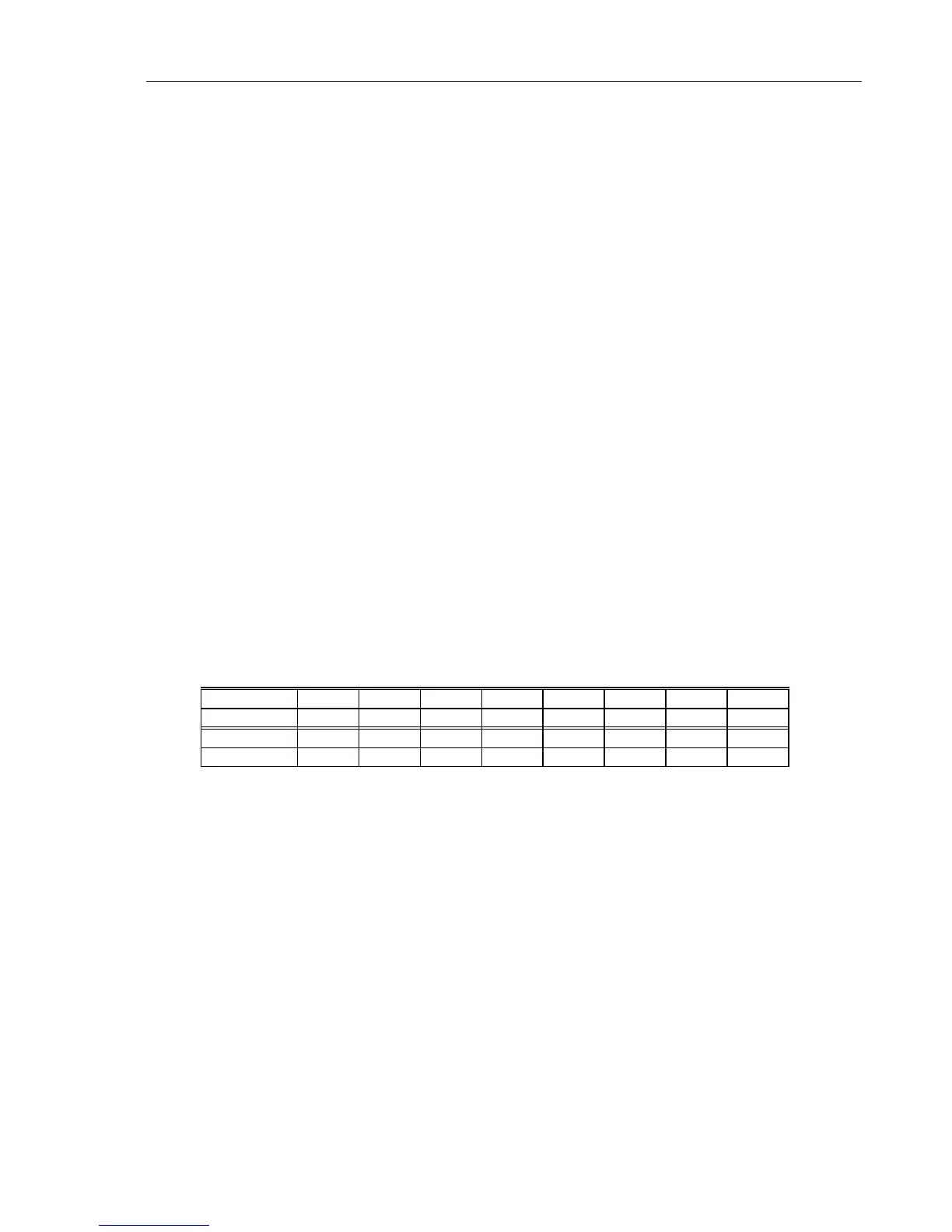
Table 3-3. shows the relation between the Input 1 reading range (V) and the trace
sensitivity (V/d.) in the Scope mode. The selected trace sensitivity determines the
C-ASIC attenuation/gain factor. The reading range is only a readout function, it does not
change the hardware range or the wave form display.
Table 3-3. Input 1 Voltage Ranges And Trace Sensitivity
range 50 mV 50 mV 50 mV 500 mV 500 mV 500 mV 5V 5V
trace ../div 5 mV 10 mV 20 mV 50 mV 100 mV 200 mV 500 mV 1V
range 5V 50V 50V 50V 500V 500V 500V 1250V
trace ../div 2V 5V 10V 20V 50V 100V 200V 500V
During measuring, input voltage measurements, gain measurements, and zero
measurements are done. As a result, the voltage supplied to the ADC is a multiplexed
(zero, + reference, -reference, input voltage) signal. In ROLL mode however, no gain
and zero measurements are done. Now the ADC input voltage includes only the
conditioned input voltage.
The input voltage is connected to Input 1. The shield of the input is connected to system
ground (⊥
⊥⊥
⊥) via a PTC ground protection resistor. If a voltage is applied between the
Input 1 and Input 2 ground shield, or between one of these ground shields and the black
COM input, the PTC resistor will limit the resulting current. The voltage across the PTC
resistor is supplied to the C-ASIC GPROT input, and causes a ground error warning
(high voltage level) on output pin 24 (DACTEST).
Input 2 Voltage Measurements
The Input 2 circuit has no HF path. The principle of operation is the same as for the
Input 1 LF path. The input ground is connected via PTC resistor R201 to the

 Loading...