-Iref
th1
th2
I-Cx
U-Cx
pos. clamp active
neg. clamp active neg. clamp active
0
0
ref clamp
TRIG-A
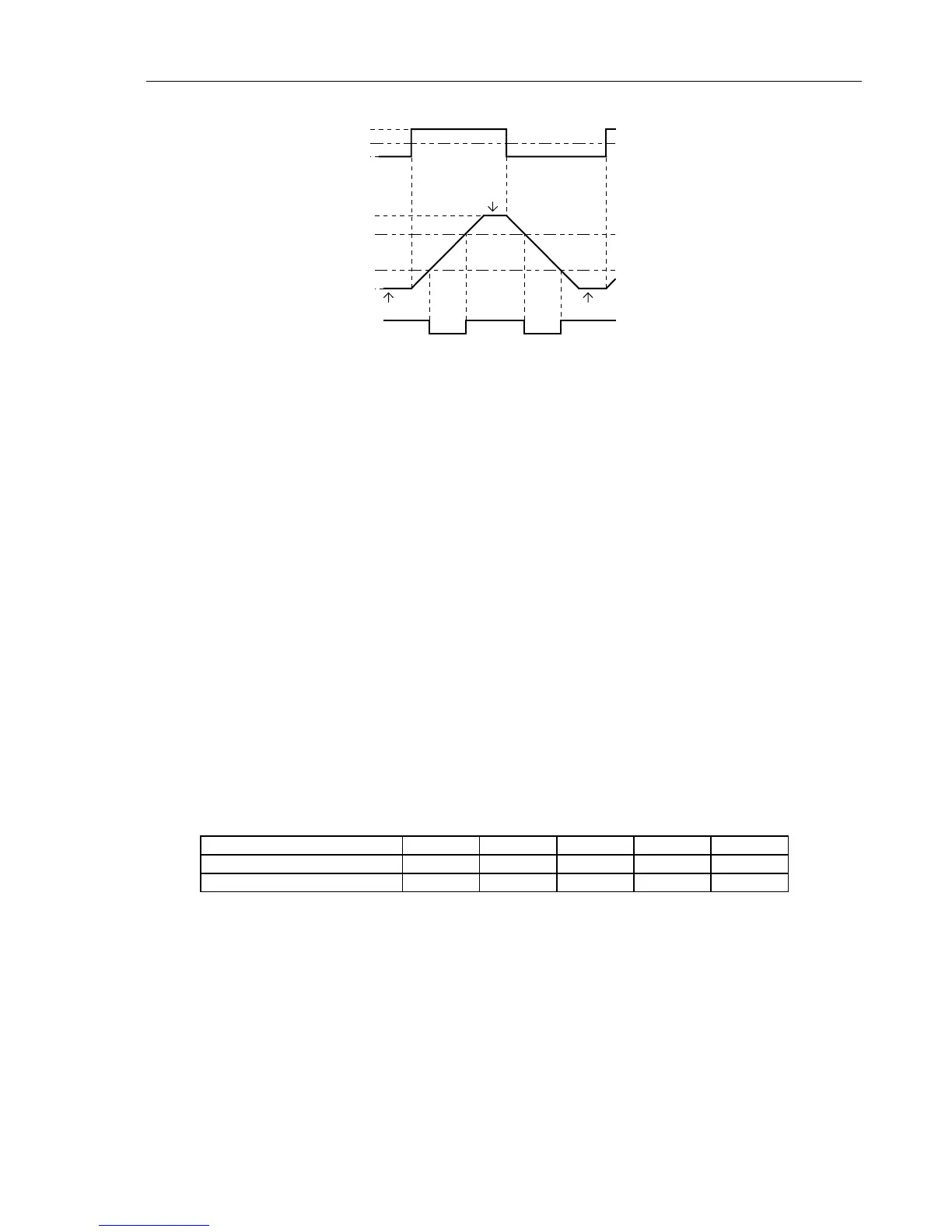
Figure 3-9. Capacitance Measurement
The T-ASIC supplies a positive (charge) and a negative (discharge) current. A
measurement cycle starts from a discharged situation (U
CX
=0) with a charge current.
After reaching the first threshold level (th
1
) the pulse width measurement is started. The
dead zone between start of charge and start of pulse width measurement avoids
measurement errors due to a series resistance of Cx.
The pulse width measurement is stopped after crossing the second threshold level (th
2
),
the completes the first part of the cycle.
Unlimited increase of the capacitor voltage is avoided by the positive clamp in the
T-ASIC. The output of the high impedance buffer in the C-ASIC supplies a replica of
the voltage across Cx to output pin 23 (ADDRESS). Via R165, this voltage is supplied
to a clamp circuit in the T-ASIC (SENSE, pin 59). This clamp circuit limits the positive
voltage on Cx to 0.45V.
Now the second part of the measurement is started by reversing the charge current. The
capacitor will be discharged in the same way as the charge cycle. The time between
passing both threshold levels is measured again. A clamp limits the minimum voltage on
Cx to 0V.
Averaging the results of both measurements cancels the effect of a possible parallel
resistance, and suppresses the influence of mains interference voltages.
Table 3-5 shows the relation between the capacitance ranges, the charge current and the
pulse width at full scale.
Table 3-5. Capacitance Ranges, Current, and Pulse Width
Range 50 nF 500 nF 5000 nF 50 µF 500 µF
Current µA0.5 µA5 µA 50 µA 500 µA 500 µA
Pulse width at Full Scale 25 ms 25 ms 25 ms 25 ms 250 ms
To protect the current source if a voltage is applied to the input, a PTC resistor R172,
and a protection circuit on the TRIGGER part, are provided (see Section 3.3.3).
Probe Detection
The Input 1 and Input 2 safety banana jacks are provided with a ground shield, consisting
of two separated half round parts. One half is connected to ground via the protection
PTC resistor R106/R206. Via a 220K resistor installed on the input block, the other half
is connected to the probe input of the D-ASIC (pin 54, 55). If the shielded STL120 test

 Loading...