43B
Service Manual
3-22
dt1
dt2
TRIGGER
SAMPLES SWEEP 1
SAMPLES SWEEP 2
3
4
21346591078 11
14
1512 13 16
PIXEL
13
14
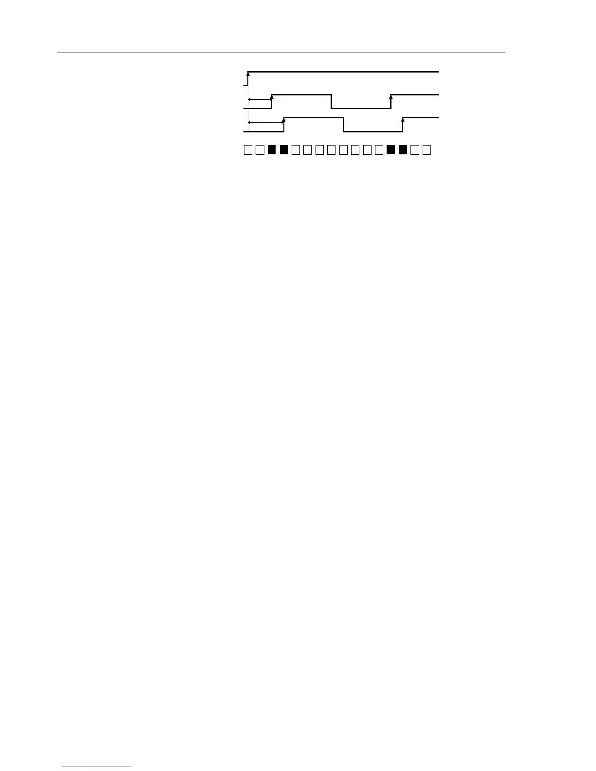
Figure 3-11. Random Repetitive Sampling Mode
DACTEST output
A frequency detector in the T-ASIC monitors the ALLTRIG signal frequency. If the
frequency is too high to obtain a reliable transmission to the D-ASIC, the DACTEST
output pin 29 will become high. The DACTEST signal is read by the D-ASIC via the
slow ADC on the Power part. It and indicates that the D-ASIC cannot use the ALLTRIG
signal (e.g. for qualified triggering).
Current Source
A current source in the T-ASIC supplies a DC current to the GENOUT output pin 1. The
current is used for resistance and capacitance measurements. It is adjustable in decades
between 50 nA and 500 µA depending on the measurement range, and is derived from an
external reference current. This reference current is supplied by the REFP reference
voltage via R323 and R324 to input REFOHMIN (pin 6).
The SENSE input signal is the buffered voltage on Input 1. For capacitance
measurements it is supplied to a clamp circuit in the T-ASIC (pin 59). The clamp circuit
limits the positive voltage on the unknown capacitance to 0.45V.
The protection circuit prevents the T-ASIC from being damaged by a voltage applied to
Input 1 during resistance or capacitance measurements. If a voltage is applied, a current
will flow via PTC resistor R172 (on the Input 1 part), V358/V359, V353, V354 to
ground. The resulting voltage across the diodes is approximately -2V or +15V.
R354/R356, and V356/V357 limit the voltage on the T-ASIC GENOUT output (pin 1).
The BOOTSTRAP output signal on pin 3 is the buffered GENOUT signal on pin 1, or
the buffered SENSE signal on pin 59. It is supplied to the protection diodes via R352,
R353, and to protection transistor V356, to minimize leakage currents.
On the ICAL-output of the T-ASIC (pin 5) a copy of the output current on GENOUT is
available. The current is supplied to the Input 1 C-ASIC via R144. As ICAL shows the
same time/temperature drift as the GENOUT measurement current, it can be used for
internal calibration of the resistance and capacitance measurement function.
Capacitor C356 is used for hum/noise suppression.

 Loading...