QUANTUM
™
HD COMPRESSOR CONTROL PANEL
MAINTENANCE
090.040-M (NOV 2016)
Page 3
LIST OF FIGURES
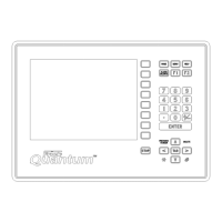
Figure 1. LCD Display Assembly & Mounting ............................. 10
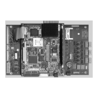
Figure 2. Q5 Processor Board Photo .........................................14
Figure 3. Interface Board Photo ................................................ 15
Figure 4. Q5 Processor Board Diagram ..................................... 16
Figure 5. Interface Board Diagram ............................................ 18
Figure 6. Pinouts and Jumper Locations .................................... 18
Figure 7. Q5 Processor Board Interconnections ........................ 19
Figure 8. Q5 Processor Board Mounting ....................................20
Figure 9. Power Supplies........................................................... 22
Figure 10. Power Supply Adjustment .......................................... 23
Figure 11. Return Lead ................................................................ 26
Figure 12. Digital Input Modules - Side View .............................. 27
Figure 13. Digital Output Module - Side View............................. 27
Figure 14. Signal Connections ..................................................... 27
Figure 15. Digital I/O Board #1 .................................................... 29
Figure 16. Digital I/O Board #2 .................................................... 30
Figure 17. Return Lead ................................................................34
Figure 18. Signal Connections ..................................................... 36
Figure 19. PHD Connections (Analog Board #1) .......................... 37
LIST OF TABLES
Table 1. Q5 Processor Board Display Jumpers .........................10
Table 2. Keyboard Mapping ..................................................... 11
Table 3. Q5 Board Jumper Settings .......................................... 17
Table 4. Q5 Board LED Denitions ........................................... 17
Table 5. Q5 Board Connector Pinouts ...................................... 17
Table 6. JP1 System Settings ................................................... 18
Table 7. Comms 1 & 2 Jumper Settings ................................... 18
Table 8. Communication Settings ............................................ 31
Table 9. Dipswitch Settings ...................................................... 31
Table 10. Analog Board Input Conguration Table ..................... 35
Table 11. Resistor Values ........................................................... 36
Table 12. Communications......................................................... 41
Table 13. Dipswitch Settings (Used to set board address) ......... 41
Table 14. Analog Board Jumper Settings ................................... 41
Table 15. Quantum HD Drawings List ........................................ 65
Table 16. Pressure Transducer Conversation Data ....................111
Table 17. Compressor Volume Ratio & Capacity Information ....112
Table 18. HD Compressor Control Replacements Parts List ......113
Table 19. Remanufactured Parts .............................................. 114
Figure 20. Current Transformer ................................................... 38
Figure 21. Analog Board #1.........................................................39
Figure 22. Analog Board #2 ........................................................40
Figure 23. USB Plug-in Locations ................................................ 49
Figure 24. Quantum HD Panel Assembly .....................................66
Figure 25. RXF Wiring Diagram (Capacity Slide Transmitter) ......70
Figure 26. RWFII Wiring Diagram (Capacity Slide Transmitter) .... 76
Figure 27. RXF/RXB Wiring Diagram (Cap. Slide Potentiometer) . 82
Figure 28. RWBII Wiring Diagram (Cap. Slide Potentiometer) ..... 88
Figure 29. RDB Wiring Diagram ..................................................94
Figure 30. PhD Wiring Diagram .................................................100
Figure 31. Digital I/O Board #2 Wiring Diagram ........................ 101
Figure 32. Analog I/O Board #2 Wiring Diagram ....................... 103
Figure 33. HD AC Power Harness .............................................. 105
Figure 33a. HD AC Power Harness (Digital Board #2) ................ 106
Figure 34. Isolater Repeater Module ......................................... 107
Figure 35. Communications Wiring Diagrams ...........................108
Figure 36. Point-To-Point Field Wiring Diagram ........................ 109