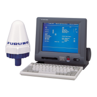
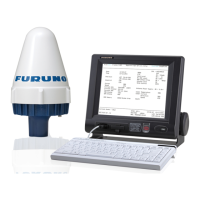
2.3 Terminal unit, IC-215
2-12
PLL and DDS circuit
DDS output is about 1.6 MHz. When transmitting, it is BPSK modulated.
Fig.2.3.7 shows the block diagram of DDS.
Fig.2.3.7 Block diagram of DDS
U4 divides it into 16 frequencies to change to about 100 kHz. About 100 kHz is mixed to
the reference oscillation frequency, 16.8 MHz to generate about 16.9 MHz. This frequency
is input to PLL OSC in U20 and divided into 42 frequencies to generate 400 kHz. This
frequency is the reference frequency of PLL synthesizer circuit, so that PLL frequency step
is 400 kHz.
Fig.2.3.8 shows the block diagram of PLL.
Fig.2.3.8 Block diagram of PLL
Before generating the standard frequency of PLL synthesizer circuit, PLL reference
frequency, that is, DDS output frequency is used based on the necessary oscillation
frequency. The used data is the frequency data sent to DDS which is 2.5 kHz step.
Fig.2.3.9 shows the frequency step of PLL and DDS.
Fig.2.3.9 Frequency step of PLL and DDS