Table of Figures
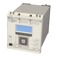
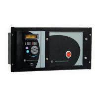
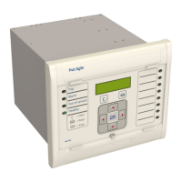
Figure 1: P40L family - version evolution 7
Figure 2: Key to logic diagrams 12
Figure 3: Functional Overview 13
Figure 4: Hardware architecture 32
Figure 5: Exploded view of IED 33
Figure 6: Front panel (40TE) 35
Figure 7: Rear view of populated case 38
Figure 8: Rear connection to terminal block 39
Figure 9: Main processor board 40
Figure 10: Power supply board 41
Figure 11: Power supply assembly 42
Figure 12: Power supply terminals 43
Figure 13: Watchdog contact terminals 44
Figure 14: Rear serial port terminals 45
Figure 15: IEC 61850-9-2LE board 45
Figure 16: Standard output relay board - 8 contacts 46
Figure 17: IRIG-B board 47
Figure 18: Fibre optic board 48
Figure 19: Rear communication board 49
Figure 20: Ethernet board 49
Figure 21: Redundant Ethernet board 51
Figure 22: Fully populated Coprocessor board 53
Figure 23: High Break relay output board 54
Figure 24: High Break contact operation 55
Figure 25: Software Architecture 60
Figure 26: Frequency response of FIR filters 66
Figure 27: Frequency Response (indicative only) 67
Figure 28: Navigating the HMI 74
Figure 29: Default display navigation 76
Figure 30: Circuit Breaker Trip Conversion Logic Diagram (Module 63) 85
Figure 31: Comparison of Conventional IED and Sampled Values IED 96
Figure 32: Data sampling using an IEC 61850-9-2LE interface 97
Figure 33: System Impedance Ratio 108
Figure 34: Directional mho element construction 111
Figure 35: Offset Mho characteristic 112
Figure 36: Directional Mho element construction – impedance domain 113
Figure 37: Offset Mho characteristics – impedance domain 114
Figure 38: Offset mho characteristics – voltage domain 115



 To Next Page