PPC600 Family Debugger | 64
©
1989-2022 Lauterbach
Mechanical Description
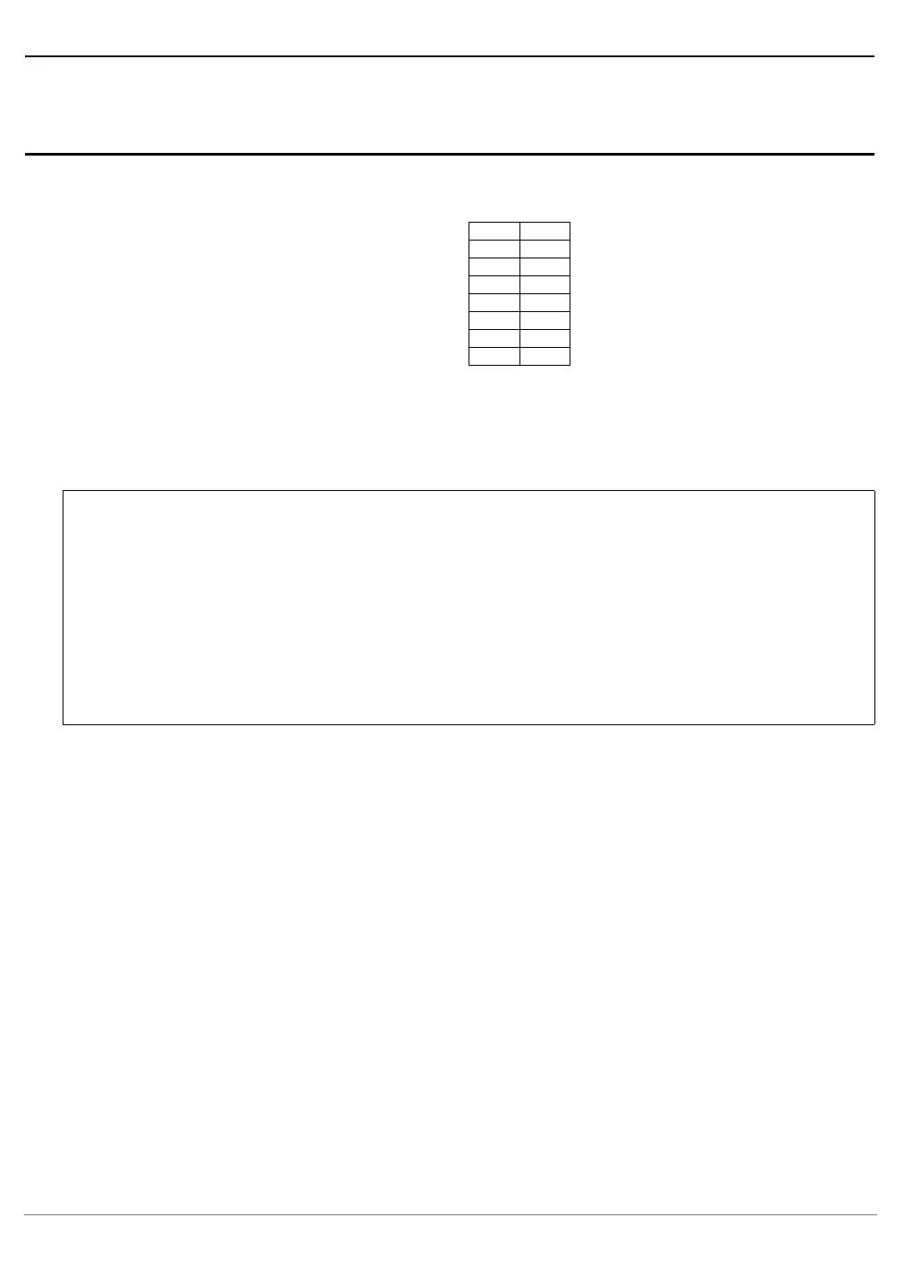
JTAG/COP Connector PPC603e/700/MPC8200
Signal Pin Pin Signal
TDO 1 2 (QACK-)
TDI 3 4 TRST-
(QREQ-) 5 6 JTAG-VREF
TCK 7 8 (PRESENT-)
TMS 9 10 N/C
(SRESET-) 11 12 GND
HRESET- 13 - N/C (KEY PIN)
(CKSTOP-) 15 16 GND
NOTE:
• This is a standard 16 pin double row (two rows of eight pins) connector (pin-
to-pin spacing: 0.100 in).
• Pin 6 (connected to VCCS) should have a resistance less than 5kOhm for
3.0~5.0V, less than 2kOhm for 1.8~3.0V.
• Pin 8 is permanently driven high (level of VCCS) by the debug cable.
• Signal in brackets are not needed by the debugger and can be left uncon-
nected.
• If CPUs have an QACK input and this input is unused, QACK should be
connected to GND. If the processor does not have QACK/QREQ pins,
leave pin 2 and 15 N/C