Page 6-6 Vector-LP Radio Beacon Transmitter Technical Instruction Manual
Issue 1.1 Section 6 Theory of Operation
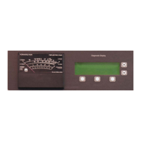
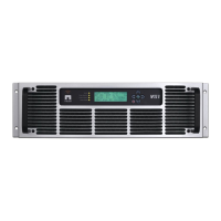
6.4 EXCITER STAGE
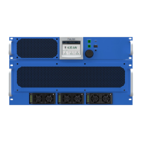
See Figures 6-2 and SD-2. In dual
configuration the exciter stage contains two
independent exciter sections (A and B) which
can be supplied in a single or a main/standby
configuration. In a main/standby
configuration, the exciter can be selected
automatically or manually by local or remote
control. Each exciter section consists of an
RF synthesizer PWB, interphase PDM driver
PWB and exciter monitor generator PWB.
6.4.1 Exciter Interface PWB
See Figures SD-9 and SD-10.The exciter
interface PWB (A2) provides signal
distribution, as well as the interconnection for
all the PWBs and assemblies in the exciter
control/monitor stage. The RF drive failure
detection, changeover/shutdown and monitor
fail logic circuits are located on the exciter
interface PWB.
6.4.1.1 RF Drive Circuitry and Failure
Detection
U3:A, U3:B, U2:A, U2:B, and U2C and their
associated components drive the RF signal to
the RF power blocks for side A. Q9 and its
associated components provide a low when
the RF drive is present and a high when it is
not present.
U3:C, U3:D, U1:A, U1:B, and U1C and their
associated components drive the RF signal to
the power blocks for side B. Q8 and its
associated components provide a low when
the RF drive is present and a high when it is
not present.
6.4.1.2 Changeover/Shutdown
U4, Q1 through Q7, K1 and K2 along with
their associated components allows for the
selection of the main side of the transmitter. If
the NDB A/B input is held low, the main side
will be B, otherwise it will be A. If no
changeover or shutdown is indicated (U4
inputs 3, 4, 6, and 7 are all high level), the
relay for the main side will be energized,
closing the contact and providing voltages to
the main PDM driver and RF synthesizer. The
relay for the standby side will be open. The
RF relay control FET (Q5) selects the main
position for RF relay K1. If a changeover is
indicated by a low on either U4:3 or U4:4, the
relay for the main side will open and the relay
for the standby side will close. The RF relay
control FET (Q5), will select the standby
position for RF relay K1. U4:17, U4:21,
U4:22, and U4:15 drive transistors Q1
through Q4 to indicate to the control board
information about the active side of the
transmitter and the changeover/ shutdown
state. If a shutdown is indicated, both K2 and
K1 are opened so that neither PDM driver or
RF synthesizer has power.
6.4.2 RF Synthesizer PWBs
See Figures SD-16 and SD-17. The RF
synthesizer PWBs (A5 and, if installed, A8)
use direct digital synthesis (DDS) to
generate carrier frequencies within the
LF/MF broadcast band (190 kHz to 1800
kHz). The output of a digital synthesizer
integrated circuit with internal high-speed
12-bit digital-to-analog converter is low-pass
filtered to provide a sinusoidal continuous
output. The sine wave is digitized and
divided by a factor of four to obtain the
carrier frequency. The digitized sine wave is
also divided by a factor of N to obtain a
2g
PDM
frequency that ultimately determines
the transmitter's pulse duration modulation
(PDM) frequency. The RF synthesizer PWB
consists of a microprocessor, direct digital
synthesizer, low pass filter, digitizer, IPM
correction, balanced drive, and N divider.
6.4.2.1 MICROPROCESSOR
The microprocessor consists of an 87C51
integrated circuit (U4), which is clocked at
the system oscillator frequency (10.0000
MHz). Firmware resides in U4's internal four
kilobytes of EPROM memory. The
microprocessor generates control
information for the DDS circuit and
generates control information for the N
divider circuit.