Electrical characteristics
MPC5777M Microcontroller Data Sheet, Rev. 6
NXP Semiconductors 89
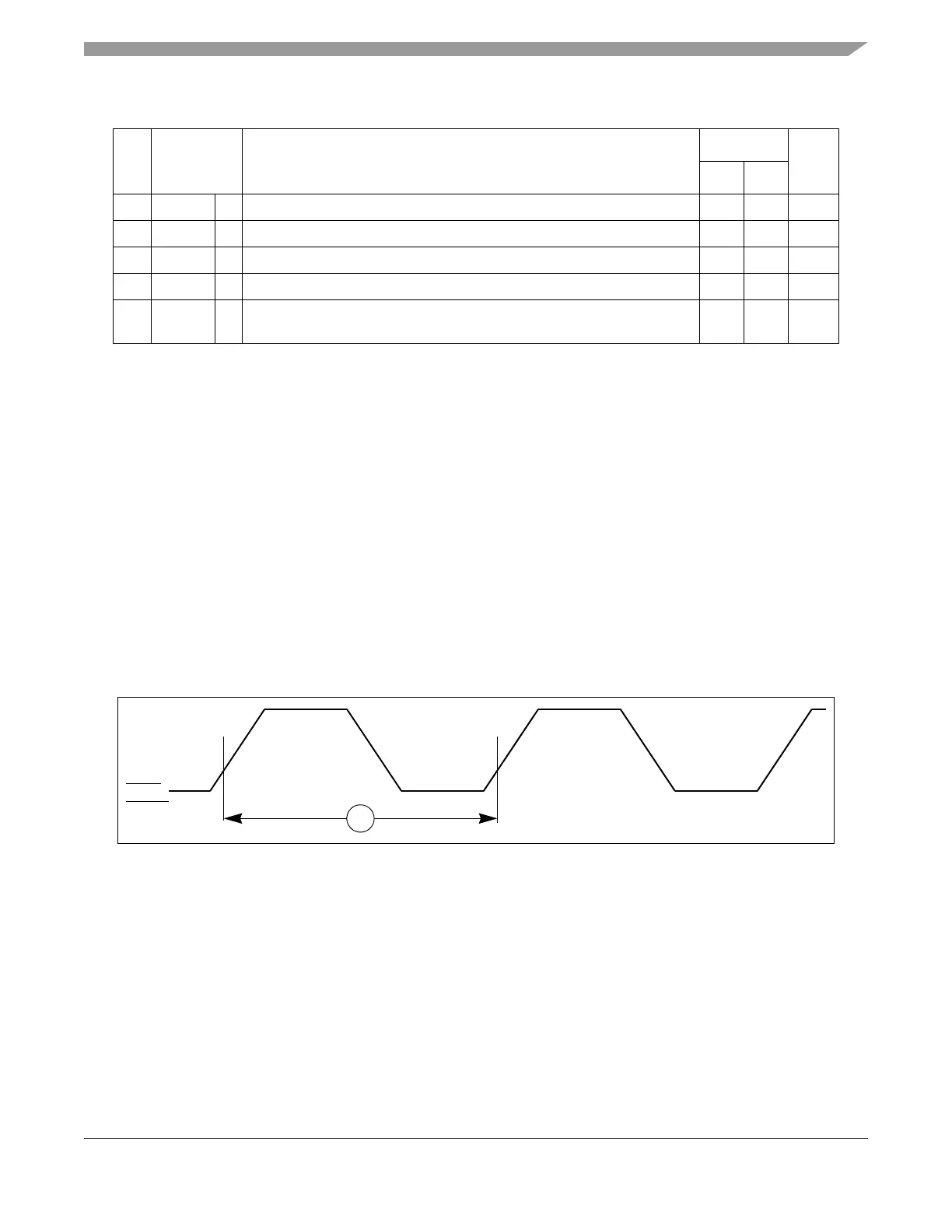
Figure 26. Nexus event trigger and test clock timings
12 t
NTDIH
CC TDI/TDIC data hold time 5 — ns
13
9
t
NTMSS
CC TMS/TMSC data setup time 5 — ns
14 t
NTMSH
CC TMS/TMSC data hold time 5 — ns
15
10
— CC TDO/TDOC propagation delay from falling edge of TCK
11
—16 ns
16 — CC TDO/TDOC hold time with respect to TCK falling edge (minimum
TDO/TDOC propagation delay)
2.25 — ns
1
Nexus timing specified at V
DD_HV_IO_JTAG
= 4.0 V to 5.5 V, and maximum loading per pad type as specified in the
I/O section of the data sheet.
2
t
CYC
is system clock period.
3
Achieving the absolute minimum TCK cycle time may require a maximum clock speed (system frequency / 8) that is
less than the maximum functional capability of the design (system frequency / 4) depending on the actual peripheral
frequency being used. To ensure proper operation TCK frequency should be set to the peripheral frequency divided
by a number greater than or equal to that specified here.
4
This is a functionally allowable feature. However, it may be limited by the maximum frequency specified by the
Absolute minimum TCK period specification.
5
This value is TDO/TDOC propagation time 36ns + 4 ns setup time to sampling edge.
6
This may require a maximum clock speed (system frequency / 8) that is less than the maximum functional capability
of the design (system frequency / 4) depending on the actual system frequency being used.
7
This value is TDO/TDOC propagation time 16ns + 4 ns setup time to sampling edge.
8
TDIC represents the TDI bit frame of the scan packet in compact JTAG 2-wire mode.
9
TMSC represents the TMS bit frame of the scan packet in compact JTAG 2-wire mode.
10
TDOC represents the TDO bit frame of the scan packet in compact JTAG 2-wire mode.
11
Timing includes TCK pad delay, clock tree delay, logic delay and TDO/TDOC output pad delay.
Table 47. Nexus debug port timing
1
(continued)
# Symbol Characteristic
Value
Unit
Min Max

 Loading...


