Electrical characteristics
MPC5777M Microcontroller Data Sheet, Rev. 6
NXP Semiconductors 109
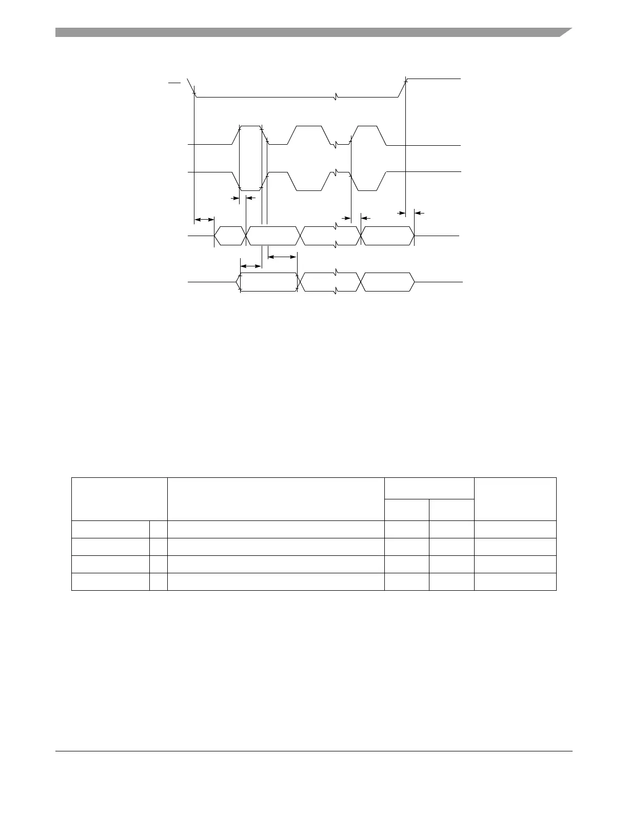
Figure 39. DSPI Slave Mode - Modified transfer format timing (MFTE = 0/1) — CPHA = 1
3.16.3 FEC timing
The FEC provides both MII and RMII interfaces in the 416 TEPBGA and 512 TEPBGA packages, and the MII and RMII
signals can be configured for either CMOS or TTL signal levels compatible with devices operating at either 5.0 V or 3.3 V.
3.16.3.1 MII receive signal timing (RXD[3:0], RX_DV, RX_ER, and RX_CLK)
The receiver functions correctly up to a RX_CLK maximum frequency of 25 MHz +1%. There is no minimum frequency
requirement. The system clock frequency must be at least equal to or greater than the RX_CLK frequency.
Table 58. MII receive signal timing
1
1
All timing specifications are referenced from RX_CLK = 1.4 V to the valid input levels, 0.8 V and 2.0 V.
Symbol Characteristic
Value
Unit
Min Max
M1 CC RXD[3:0], RX_DV, RX_ER to RX_CLK setup 5 — ns
M2 CC RX_CLK to RXD[3:0], RX_DV, RX_ER hold 5 — ns
M3 CC RX_CLK pulse width high 35% 65% RX_CLK period
M4 CC RX_CLK pulse width low 35% 65% RX_CLK period
Last Data
Last Data
SIN
SOUT
SS
First Data
First Data
Data
Data
SCK Input
SCK Input
(CPOL=0)
(CPOL=1)
t
A
t
DIS
t
SUI
t
HI
t
SUO
t
HO

 Loading...


