Electrical characteristics
MPC5777M Microcontroller Data Sheet, Rev. 6
NXP Semiconductors 53
3.10.2 SAR ADC electrical specification
The SARn ADCs are 12-bit Successive Approximation Register analog-to-digital converters with full capacitive DAC. The
SARn architecture allows input channel multiplexing.
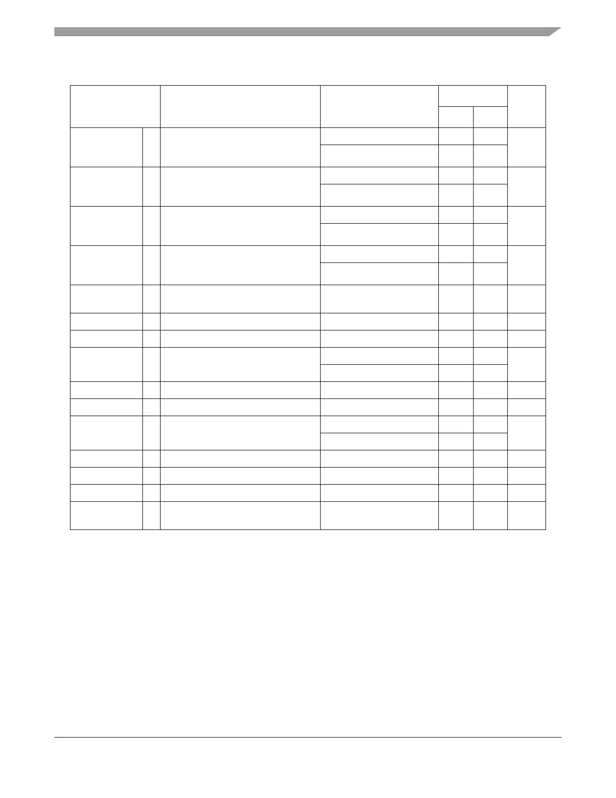
Table 26. ADC pin specification
1
1
All specifications in this table valid for the full input voltage range for the analog inputs.
Symbol Parameter Conditions
Value
Unit
Min Max
I
LK_INUD
CC Input leakage current, two ADC
channels input with weak pull-up and
weak pull-down
T
J
< 40 °C — 50 nA
T
J
< 150 °C — 150
I
LK_INUSD
CC Input leakage current, two ADC
channels input with weak pull-up and
strong pull-down
T
J
< 40 °C — 80 nA
T
J
< 150 °C — 250
I
LK_INREF
CC Input leakage current, two ADC
channels input with weak pull-up and
weak pull-down and alternate reference
T
J
<40°C — 160 nA
T
J
< 150 °C — 400
I
LK_INOUT
CC Input leakage current, two ADC
channels input, GPIO output buffer with
weak pull-up and weak pull-down
T
J
<40°C — 140 nA
T
J
< 150 °C — 380
I
INJ
CC Injection current on analog input
preserving functionality
Applies to any analog pins –3 3 mA
C
HV_ADC
SR V
DD_HV_ADV
external capacitance
2
2
For noise filtering, add a high frequency bypass capacitance of 0.1 µF between V
DD_HV_ADV
and V
SS_HV_ADV
.
12.2µF
C
P1
CC Pad capacitance — 0 10 pF
C
P2
CC Internal routing capacitance SARn channels 0 0.5 pF
SARB channels 0 1
C
P3
CC Internal routing capacitance Only for SARB channels 0 1 pF
C
S
CC SAR ADC sampling capacitance — 6 8.5 pF
R
SWn
CC Analog switches resistance SARn channels 0 1.1 k
SARB channels 0 1.7
R
AD
CC ADC input analog switches resistance — 0 0.6 k
R
CMSW
CC Common mode switch resistance — 0 2.6 k
R
CMRL
CC Common mode resistive ladder — 0 3.5 k
R
SAFEPD
3
3
Safety pull-down is available for port pin PB[5] and PE[14].
CC Discharge resistance for AN7/AN35
channels (strong pull-down for safety)
—0300

 Loading...


