MPC5777M Microcontroller Data Sheet, Rev. 6
Electrical characteristics
NXP Semiconductors108
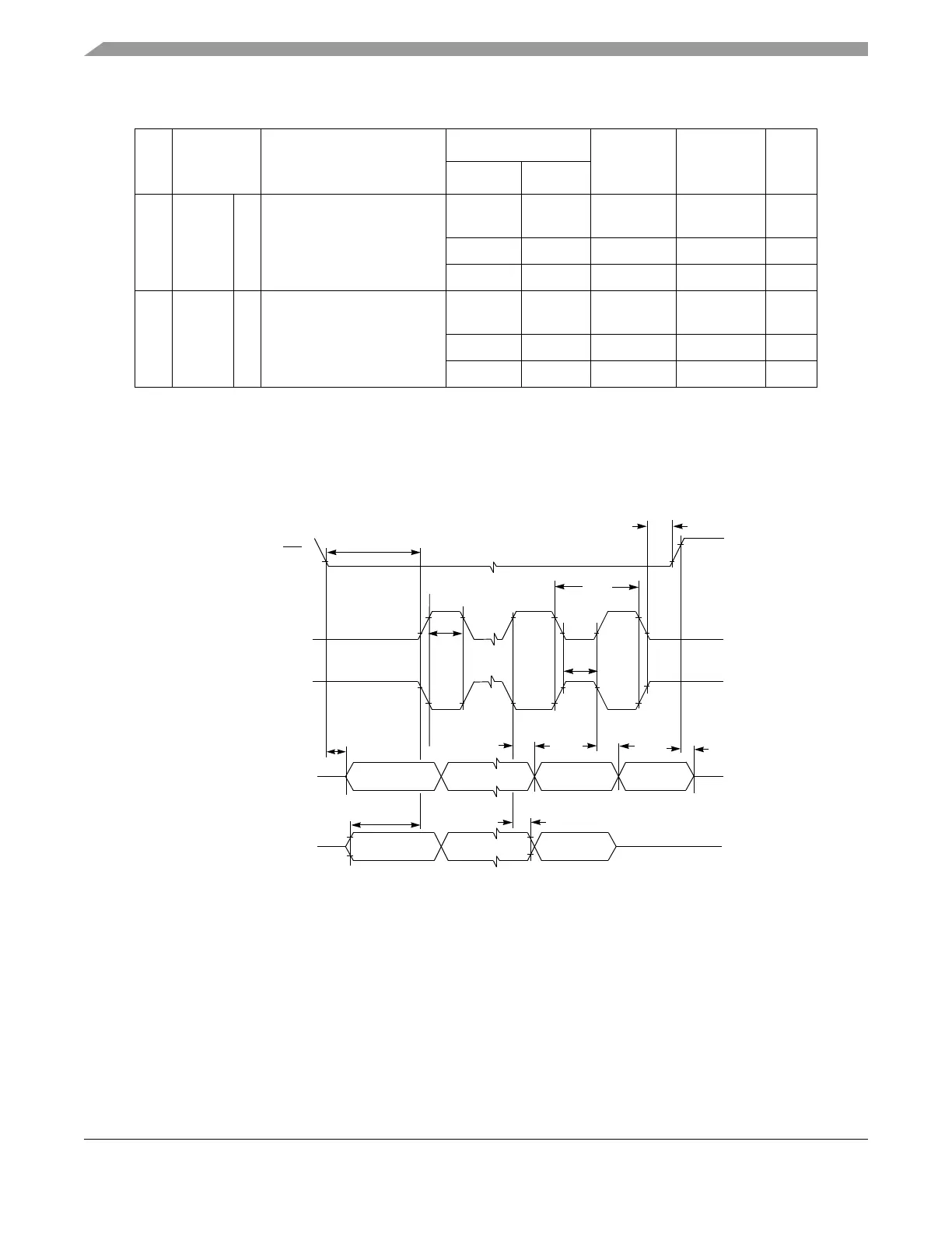
Figure 38. DSPI Slave Mode - Modified transfer format timing (MFTE = 0/1) — CPHA = 0
11 t
SUO
CC SOUT Valid Time
2,3,4
(after SCK edge)
Very
Strong
25 pF — 30 ns
Strong 50 pF — 30 ns
Medium 50 pF — 50 ns
12 t
HO
CC SOUT Hold Time
2,3,4
(after SCK edge)
Very
Strong
25 pF 2.5 —ns
Strong 50 pF 2.5 —ns
Medium 50 pF 2.5 —ns
1
DSPI slave operation is only supported for a single master and single slave on the device. Timing is valid for
that case only.
2
Input timing assumes an input slew rate of 1 ns (10% - 90%) and uses TTL / Automotive voltage thresholds.
3
All timing values for output signals in this table, are measured to 50% of the output voltage.
4
All output timing is worst case and includes the mismatching of rise and fall times of the output pads.
Table 57. DSPI CMOS Slave timing - Modified Transfer Format (MTFE = 0/1)
1
# Symbol Characteristic
Condition
Min Max Unit
Pad Drive Load
Last Data
First Data
Data
Data
SIN
SOUT
SS
SCK Input
First Data
Last Data
SCK Input
(CPOL=0)
(CPOL=1)
t
SCK
t
A
t
DIS
t
SDC
t
SDC
t
CSC
t
ASC
t
SUI
t
HI
t
SUO
t
HO

 Loading...


