Operating Instructions Chapter 11
C 4000 Standard/Advanced
8 009 861/OE59/19-11-04 © SICK AG • Industrial Safety Systems • Germany • All rights reserved
67
Technical specifications
" Receiver unit
Switching outputs (OSSDs) 2 PNP semiconductor, short-circuit protected
4)
,
cross-circuit monitored
Response time See chapter 11.2 on page 69
Switch off time 100 ms
Switch on time 2.5 × response
time (single
system)
4.5 × response
time (cascade)
Switching voltage
5)
6)
HIGH
(active, U
eff
)
U
V
– 2.25 V 24 V U
V
Switching voltage
5)
LOW
(inactive)
0 V 0 V 3.5 V
Switching current 0 mA 500 mA
Leakage current
7)
0.25 mA
Load capacity 2.2 µF
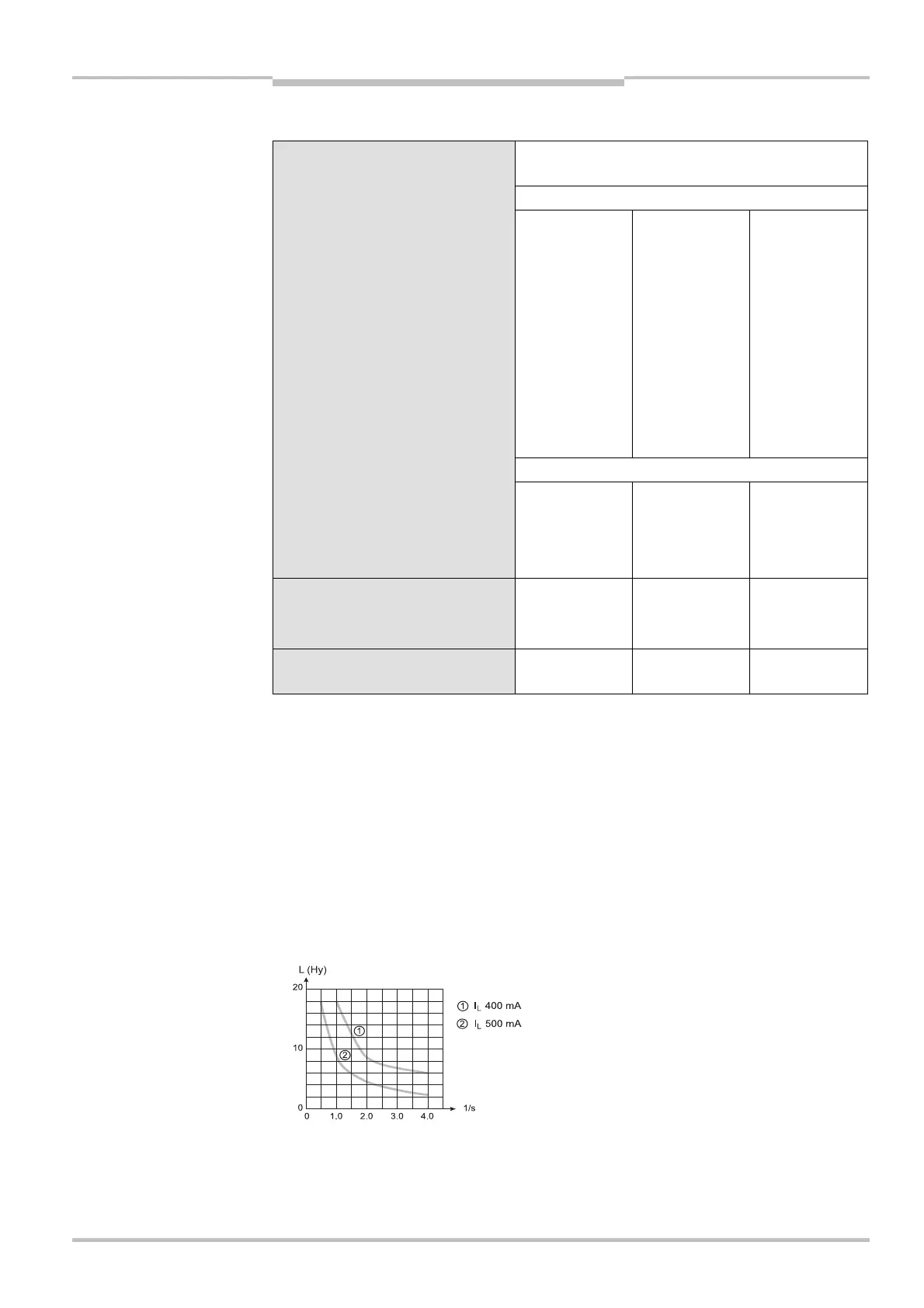
Switching sequence Depending on load inductance
Load inductance
8)
2.2 H
Test pulse data
9)
Test pulse width 120 µs 150 µs 300 µs
Test pulse rate 3
1
/s 5
1
/s 10
1
/s
Permissible line resistance
between device and load
10)
2.5 '
Supply lead 1 '
Power consumption 3 A (host/
guest/guest)
4)
Applies to the voltage range between –30 V and +30 V.
5)
As per IEC 61)131-2.
6)
On the device plug.
7)
In the case of a fault (0-V cable open circuit) the max. leakage current flows in the OSSD cable. The down-
stream controller must detect this status as LOW. A FPLC (Fail-safe Programmable Logic Controller) must be
able to identify this status.
8)
The maximum rated load inductance is higher with lower switching sequence.
9)
When active, the outputs are tested cyclically (brief LOW). When selecting the downstream controllers, make
sure that the test pulses do not result in deactivation when using the above parameters.
10)
Make sure to limit the individual line core resistance to the downstream controller to this value to ensure that
a short-circuit between the outputs is safely detected. (Also note EN 60))204 Electrical Machine Equipment,
Part 1: General Requirements.)