HAP-S1
HAP-S1
4545
For Schematic Diagrams.
Note:
• All capacitors are in μF unless otherwise noted. (p: pF) 50
WV or less are not indicated except for electrolytics and
tantalums.
• All resistors are in Ω and 1/4 W or less unless otherwise
specifi ed.
•
f
: Internal component.
• 2 : Nonfl ammable resistor.
• C : Panel designation.
THIS NOTE IS COMMON FOR PRINTED WIRING BOARDS AND SCHEMATIC DIAGRAMS.
(In addition to this, the necessary note is printed in each block.)
• A : B+ Line.
• B : B– Line.
• Voltages and waveforms are dc with respect to ground
under no-signal conditions.
no mark
: POWER ON
• Voltages are taken with VOM (Input impedance 10 M).
Voltage variations may be noted due to normal production
tolerances.
• Waveforms are taken with a oscilloscope.
Voltage variations may be noted due to normal production
tolerances.
• Circled numbers refer to waveforms.
• Signal path.
F : AUDIO (ANALOG)
J : AUDIO (DIGITAL)
L : AUDIO IN (ANALOG)
c : AUDIO IN (DIGITAL)
f : HDD
N : USB
d : LAN
G : WIRELESS LAN
E : VIDEO
• The voltage and waveform of CSP (chip size package)
cannot be measured, because its lead layout is different
from that of conventional IC.
• Abbreviation
CND : Canadian model
For Printed Wiring Boards.
Note:
• X : Parts extracted from the component side.
• Y : Parts extracted from the conductor side.
•
f
: Internal component.
• : Pattern from the side which enables seeing.
(The other layers’ patterns are not indicated.)
Caution:
Pattern face side:
(SIDE B)
Parts face side:
(SIDE A)
Parts on the pattern face side seen
from the pattern face are indicated.
Parts on the parts face side seen from
the parts face are indicated.
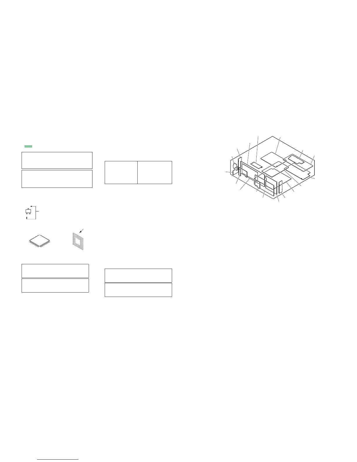
• Circuit Boards Location
• Indication of transistor.
C
B
These are omitted.
E
Q
Caution:
Pattern face side:
(Conductor Side)
Parts face side:
(Component Side)
Parts on the pattern face side seen
from the pattern face are indicated.
Parts on the parts face side seen from
the parts face are indicated.
Note:
The components identi-
fi ed by mark 0 or dotted
line with mark 0 are criti-
cal for safety.
Replace only with part
number specifi ed.
Note:
Les composants identifi és
par une marque 0 sont
critiques pour la sécurité.
Ne les remplacer que par
une pièce portant le nu-
méro spécifi é.
• Abbreviation
CND : Canadian model
• FPGA DSP and MAIN boards are multi-layer printed
board. However, the patterns of intermediate layers have
not been included in diagrams.
• Lead layouts
surface
CSP (Chip Size Package) Lead layout of conventional IC
Note 1: When the complete MAIN board is replaced, refer to
“NOTE OF REPLACING THE COMPLETE MAIN
BOARD” and “CHECKING METHOD OF NET-
WORK CONNECTION” on page 5.
Note 2: When the complete AMP board is replaced, refer to
“NOTE OF REPLACING THE D218, IC350 AND
IC351 ON THE AMP BOARD AND THE COM-
PLETE AMP BOARD” on page 4.
SPTM board
DIGITAL IO board
DCDC board
DAC board
AMP board
STANBY board
ALLEGRO-ANT-L board
MAIN board
WLAN/BT COMBO card
(WBC1)
ALLEGRO-ANT-L board
U-COM board
HP board
ALLEGRO-LCD board
POWER KEY board
KEY JOG board
PENC board
FPGA DSP board

 Loading...