EasyManua.ls Logo

Tegam 1750 - Page 56

Tegam 1750
76 pages
Print Icon
To Next Page IconTo Next Page
To Previous Page IconTo Previous Page
Loading...
10 TEGAM WAY • GENEVA, OHIO 44041 • 440-466-6100 • FAX 440-466-6110 • sales@tegam.com
5-15
PROGRAMMING AND INTERFACING
IEEE-488.1 OPERATION
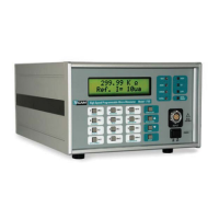
The Model 1750 may operate in either GPIB or RS232 communication interface. From the factory, the
1750 is configured for GPIB communication at address 12. To change the GPIB address, select
[MENU]>[INTERFACE]>[GPIB]>[ENTER]. You will be prompted to enter a new GPIB address. Type in
the new GPIB address and press [ENTER]. The new GPIB setting is now activated.
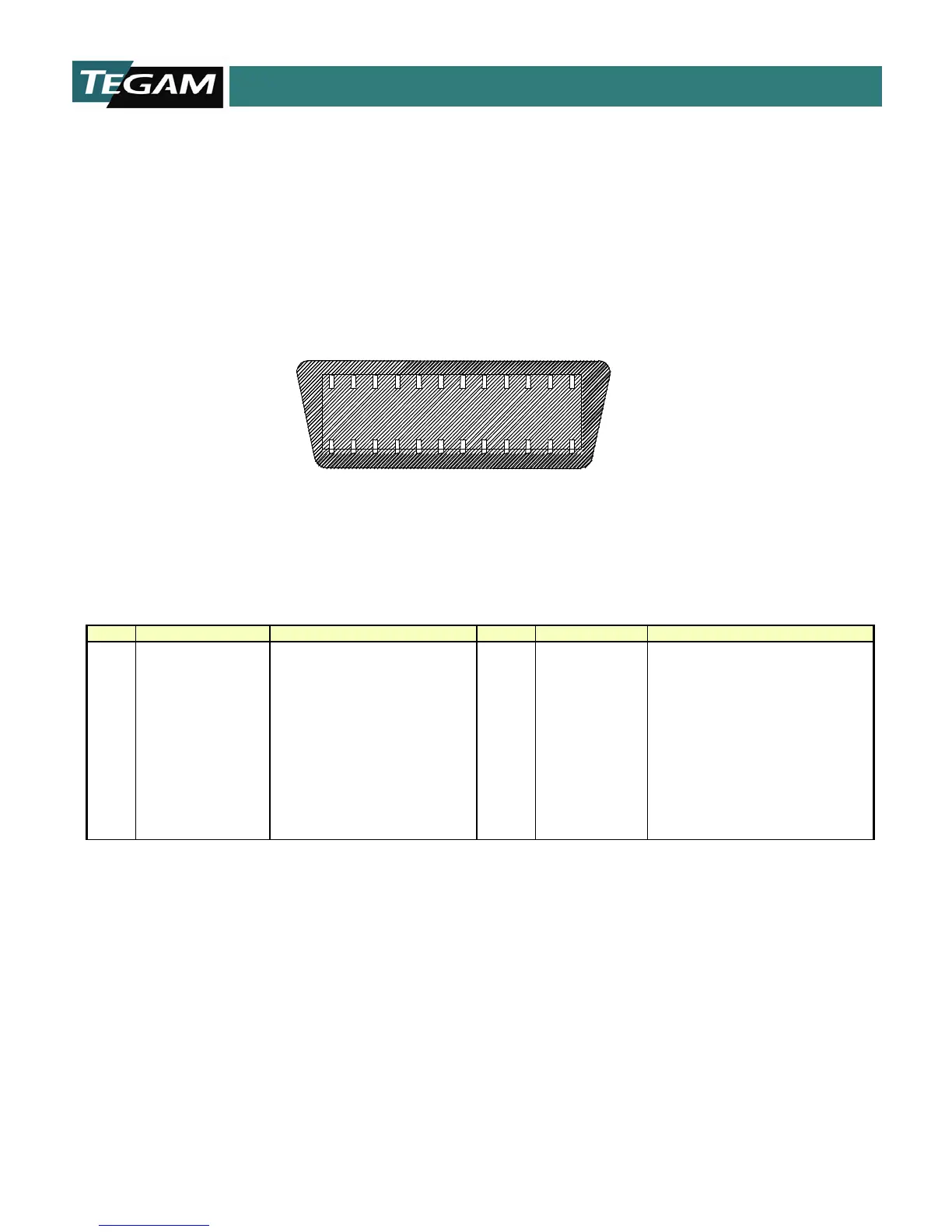
Below is an illustration of the rear panel GPIB connector and a definition of the pin assignments can
be found in the table below.
`
Figure 5.5: GPIB Connector
Pin
Signal
Function
Pin
Signal
Function
1
DIO1
Data input/ output bit 1
13
DIO5
Data input/ output bit 5
2
DIO2
Data input/ output bit 2
14
DIO6
Data input/ output bit 6
3
DIO3
Data input/ output bit 3
15
DIO7
Data input/ output bit 7
4
DIO4
Data input/ output bit 4
16
DIO8
Data input/ output bit 8
5
EOI
End or identity
17
REN
Remote Enable
6
DAV
Data Valid
18
SHIELD
Ground (DAV)
7
NRFD
Not Ready for Data
19
SHIELD
Ground (NRFD)
8
NDAC
Not Data Accepted
20
SHIELD
Ground (NDAC)
9
IFC
Interface Clear
21
SHIELD
Ground (IFC)
10
SRQ
Service request
22
SHIELD
Ground (SRQ)
11
ATN
Attention
23
SHIELD
Ground (ATN)
12
SHIELD
Chassis Ground
24
SIGNAL GND
Signal Ground
Table 5.5: Pin Outs for GPIB Rear Connector
1
12
13
24
Rear Panel View

Table of Contents

Related product manuals