Maintenance—2230 Service
If there were power-up faults:
Display the power-up faults on U4119.
Display the power-up faults on the crt without
maskable interrupt support:
Until a Menu button is changed.
Start normal instrument operation.
Diagnostic Tests
PU TEST. At power-up, this kernel test does a quick
check of the instruments dynamic RAM (random access
memory), ROM (read only memory), and NMI (non
maskable interrupt) circuitry. If no errors are found,
additional diagnostic tests are run.
If errors are found, their code is displayed (at power-up
before NMI or Ml go HI and’ before other tests are run)
repeatedly, for approximately 2 sec, on U4113 and U4119
(see Table 6-13). The instrument also tries to display the
errors on the crt as a four digit hexadecimal number:
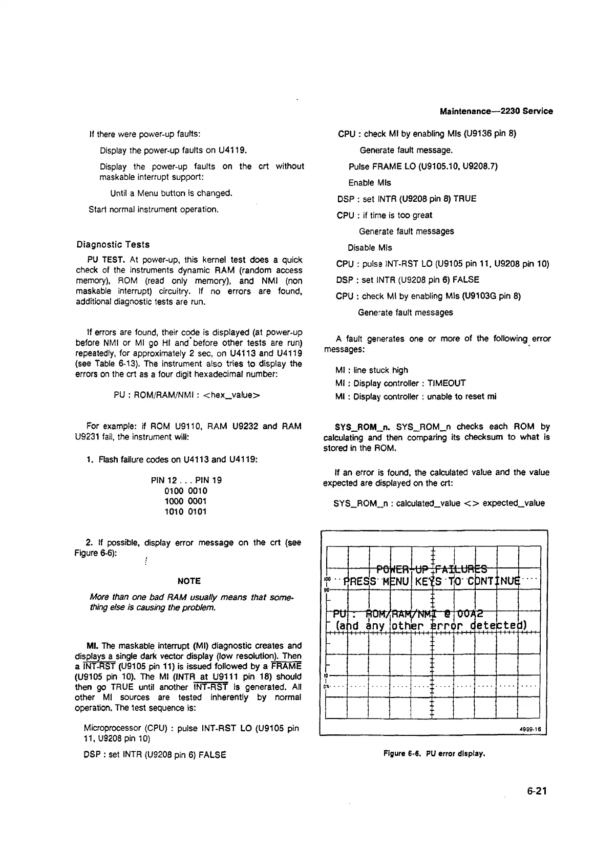
PU : ROM/RAM/NMI : <hex_value>
CPU : check Ml by enabling Mis (U9136 pin 8)
Generate fault message.
Pulse FRAME LO (U9105.10, U9208.7)
Enable Mis
DSP : set INTR (U9208 pin 8) TRUE
CPU : if time is too great
Generate fault messages
Disable Mis
CPU : pulse INT-RST LO (U9105 pin 11, U9208 pin 10)
DSP : set INTR (U9208 pin 6) FALSE
CPU : check Ml by enabling Mis (U9103G pin 8)
Generate fault messages
A fault generates one or more of the following error
messages:
M l: line stuck high
M l: Display controller: TIMEOUT
M l: Display controller: unable to reset mi
For example: if ROM U9110, RAM U9232 and RAM SYS_ROM„n. SYS_ROM_n checks each ROM by
U9231 fail, the instrument will: calculating and then comparing its checksum to what is
stored in the ROM.
1. Flash failure codes on U4113 and U4119:
PIN 12 .. . PIN 19
0100 0010
1000 0001
1010 0101
If an error is found, the calculated value and the value
expected are displayed on the crt:
SYS_ROM„n : calculated_value < > expected_value
2. If possible, display error message on the crt (see
Figure 6-6):
NOTE
More than one bad RAM usually means that some
thing else is causing the problem.
Ml. The maskable interrupt (Ml) diagnostic creates and
displays a single dark vector display (low resolution). Then
a INT-RST (U9105 pin 11) is issued followed by a FRAME
(U9105 pin 10). The Ml (INTR at U9111 pin 18) should
then go TRUE until another INT-RST is generated. All
other Ml sources are tested inherently by normal
operation. The test sequence is:
Microprocessor (CPU) : pulse INT-RST LO (U9105 pin
11, U9208 pin 10)
DSP : set INTR (U9208 pin 6) FALSE
7 • ■ f
RES
“ TO
S M
TCn*
ENU
KEi
tr A I
IS T
L u n
0 ' C
ib
d n t ;:nue
PU
' (a
: "f
id <
TOM7
*ny
RAM
O th
/NM-
BP 3
[ @
;r r c
"OOA
IP (C
2
e te
c te
J ) ,.
-
-
OT
499 9-16
6-21
Figure 6-6. PU error display.