Theory of Operation—2230 Service
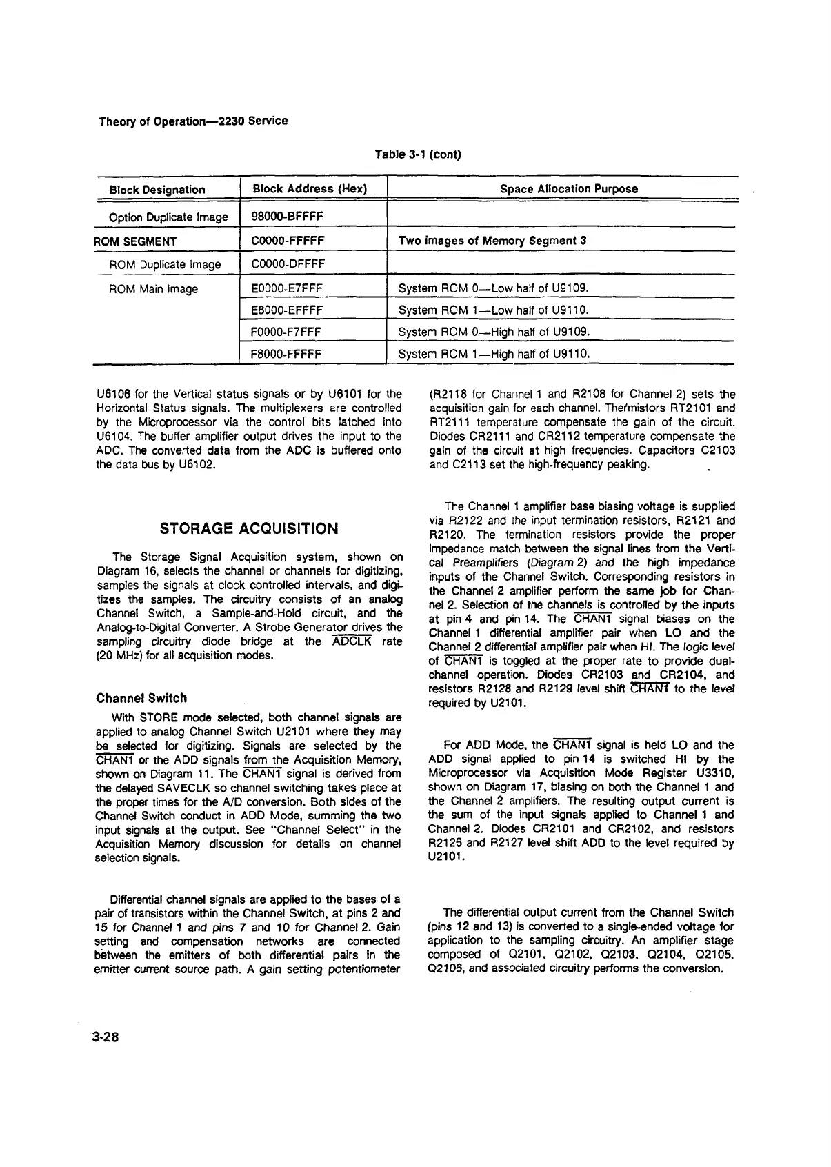
Table 3-1 (cont)
Block Designation
Block Address (Hex)
Space Allocation Purpose
Option Duplicate Image
98000-BFFFF
ROM SEGMENT
C0000-FFFFF
Two images of Memory Segment 3
ROM Duplicate Image
C0000-DFFFF
ROM Main Image
E0000-E7FFF
System ROM 0—Low half of U9109.
E8000-EFFFF
System ROM 1—Low half of U9110.
F0000-F7FFF
System ROM 0—High half of U9109.
F8000-FFFFF
System ROM 1—High half of U9110.
U6106 for the Vertical status signals or by U6101 for the
Horizontal Status signals. The multiplexers are controlled
by the Microprocessor via the control bits latched into
U6104. The buffer amplifier output drives the input to the
ADC. The converted data from the ADC is buffered onto
the data bus by U6102.
STORAGE ACQUISITION
The Storage Signal Acquisition system, shown on
Diagram 16, selects the channel or channels for digitizing,
samples the signals at clock controlled intervals, and digi
tizes the samples. The circuitry consists of an analog
Channel Switch, a Sample-and-Hold circuit, and the
Analog-to-Digital Converter. A Strobe Generator drives the
sampling circuitry diode bridge at the ADCLK rate
(20 MHz) for all acquisition modes.
Channel Switch
With STORE mode selected, both channel signals are
applied to analog Channel Switch U2101 where they may
be selected for digitizing. Signals are selected by the
CHAN1 or the ADD signals from the Acquisition Memory,
shown on Diagram 11. The CHAN1 signal is derived from
the delayed SAVECLK so channel switching takes place at
the proper times for the A/D conversion. Both sides of the
Channel Switch conduct in ADD Mode, summing the two
input signals at the output. See “Channel Select” in the
Acquisition Memory discussion for details on channel
selection signals.
Differential channel signals are applied to the bases of a
pair of transistors within the Channel Switch, at pins 2 and
15 for Channel 1 and pins 7 and 10 for Channel 2. Gain
setting and compensation networks are connected
between the emitters of both differential pairs in the
emitter current source path. A gain setting potentiometer
(R2118 for Channel 1 and R2108 for Channel 2) sets the
acquisition gain for each channel. Thermistors RT2101 and
RT2111 temperature compensate the gain of the circuit.
Diodes CR2111 and CR2112 temperature compensate the
gain of the circuit at high frequencies. Capacitors C2103
and C2113 set the high-frequency peaking.
The Channel 1 amplifier base biasing voltage is supplied
via R2122 and the input termination resistors, R2121 and
R2120. The termination resistors provide the proper
impedance match between the signal lines from the Verti
cal Preamplifiers (Diagram 2) and the high impedance
inputs of the Channel Switch. Corresponding resistors in
the Channel 2 amplifier perform the same job for Chan
nel 2. Selection of the channels is controlled by the inputs
at pin 4 and pin 14. The CHAN1 signal biases on the
Channel 1 differential amplifier pair when LO and the
Channel 2 differential amplifier pair when HI. The logic level
of CHAN1 is toggled at the proper rate to provide dual
channel operation. Diodes CR2103 and CR2104, and
resistors R2128 and R2129 level shift CHAN1 to the level
required by U2101.
For ADD Mode, the CHAN1 signal is held LO and the
ADD signal applied to pin 14 is switched HI by the
Microprocessor via Acquisition Mode Register U3310,
shown on Diagram 17, biasing on both the Channel 1 and
the Channel 2 amplifiers. The resulting output current is
the sum of the input signals applied to Channel 1 and
Channel 2. Diodes CR2101 and CR2102, and resistors
R2126 and R2127 level shift ADD to the level required by
U2101.
The differential output current from the Channel Switch
(pins 12 and 13) is converted to a single-ended voltage for
application to the sampling circuitry. An amplifier stage
composed of Q2101, Q2102, Q2103, Q2104, Q2105,
Q2106, and associated circuitry performs the conversion.
3-28