SPICLK
(clock polarity=0)
SPISIMO
SPICSn
Master Out Data Is Valid
9
SPICLK
(clock polarity=1)
SPIENAn
10
Write to buffer
11
8
SPISOMI
SPISIMO
SPICLK
(clock polarity = 1)
SPICLK
(clock polarity = 0)
Data Valid
Master In Data
Must Be Valid
Master Out Data Is Valid
3
2
1
5
4
7
6
139
TMS570LS0714
www.ti.com
SPNS226E –JUNE 2013–REVISED NOVEMBER 2016
Submit Documentation Feedback
Product Folder Links: TMS570LS0714
Peripheral Information and Electrical SpecificationsCopyright © 2013–2016, Texas Instruments Incorporated
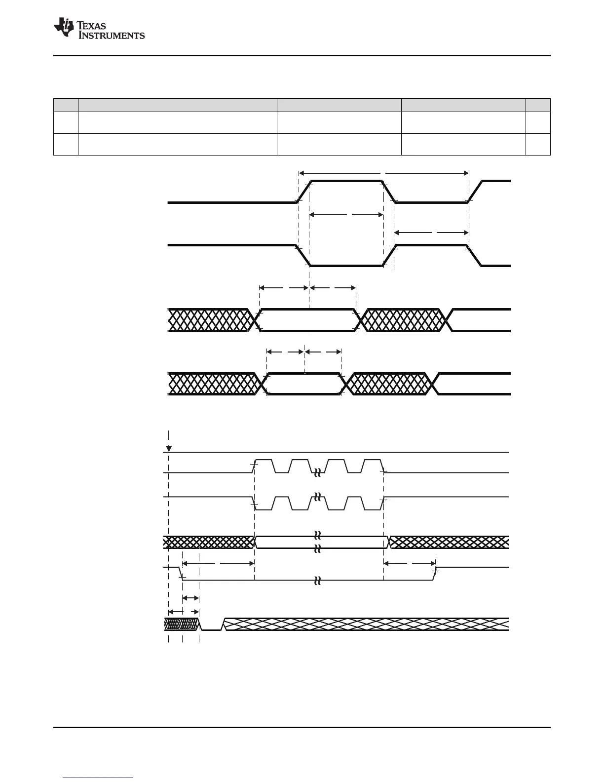
Table 7-37. SPI Master Mode External Timing Parameters (CLOCK PHASE = 1, SPICLK = output,
SPISIMO = output, and SPISOMI = input)
(1)(2)(3)
(continued)
NO. PARAMETER MIN MAX UNIT
10 t
SPIENA
SPIENAn Sample Point
(C2TDELAY+1)* t
c(VCLK)
-
t
f(SPICS)
– 29
(C2TDELAY+1)*t
c(VCLK)
ns
11 t
SPIENAW
SPIENAn Sample point from write
to buffer
(C2TDELAY+2)*t
c(VCLK)
ns
Figure 7-22. SPI Master Mode External Timing (CLOCK PHASE = 1)
Figure 7-23. SPI Master Mode Chip-Select Timing (CLOCK PHASE = 1)
 Loading...


