/NR
/1 to /64
OSCIN
PLL
INTCLK
/OD
/1 to /8
VCOCLK
/R
/1 to /32
post_ODCLK
/NF
/1 to /256
PLLCLK
f
PLLCLK
= (f
OSCIN
/ NR) * NF / (OD * R)
53
TMS570LS0714
www.ti.com
SPNS226E –JUNE 2013–REVISED NOVEMBER 2016
Submit Documentation Feedback
Product Folder Links: TMS570LS0714
System Information and Electrical SpecificationsCopyright © 2013–2016, Texas Instruments Incorporated
6.6.1.2.2 LPO Electrical and Timing Specifications
Table 6-10. LPO Specifications
PARAMETER MIN TYP MAX UNIT
Clock detection Oscillator fail frequency - lower threshold, using untrimmed
LPO output
1.375 2.4 4.875 MHz
Oscillator fail frequency - higher threshold, using untrimmed
LPO output
22 38.4 78 MHz
LPO - HF oscillator Untrimmed frequency 5.5 9 19.5 MHz
Trimmed frequency 8 9.6 11 MHz
Start-up time from STANDBY (LPO BIAS_EN high for at
least 900 µs)
10 µs
Cold start-up time 900 µs
LPO - LF oscillator Untrimmed frequency 36 85 180 kHz
Start-up time from STANDBY (LPO BIAS_EN high for at
least 900 µs)
100 µs
Cold start-up time 2000 µs
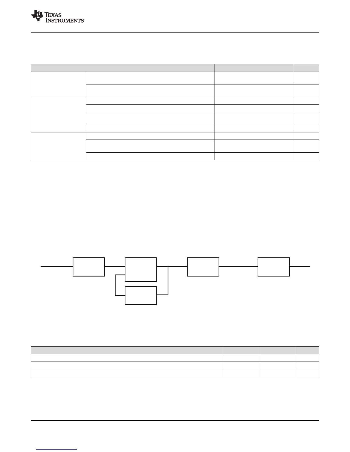
6.6.1.3 Phase-Locked Loop (PLL) Clock Module
The PLL is used to multiply the input frequency to some higher frequency.
The main features of the PLL are:
• Frequency modulation can be optionally superimposed on the synthesized frequency of PLL1.
• Configurable frequency multipliers and dividers
• Built-in PLL Slip monitoring circuit
• Option to reset the device on a PLL slip detection
6.6.1.3.1 Block Diagram
Figure 6-6 shows a high-level block diagram of the PLL macro on this microcontroller.
Figure 6-6. PLL Block Diagram
6.6.1.3.2 PLL Timing Specifications
Table 6-11. PLL Timing Specifications
PARAMETER MIN MAX UNIT
f
INTCLK
PLL1 Reference Clock frequency 1 20 MHz
f
post_ODCLK
Post-ODCLK – PLL1 Post-divider input clock frequency 400 MHz
f
VCOCLK
VCOCLK – PLL1 Output Divider (OD) input clock frequency 150 550 MHz
 Loading...


