59
TMS570LS0714
www.ti.com
SPNS226E –JUNE 2013–REVISED NOVEMBER 2016
Submit Documentation Feedback
Product Folder Links: TMS570LS0714
System Information and Electrical SpecificationsCopyright © 2013–2016, Texas Instruments Incorporated
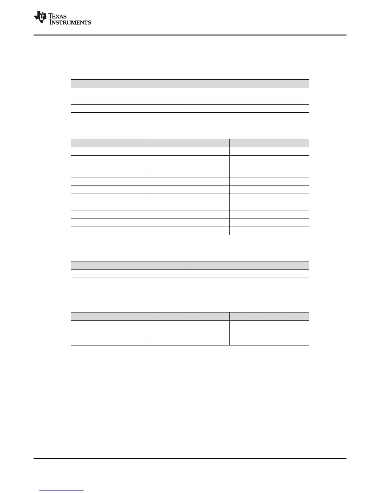
6.7.3.2 Mapping of DCC Clock Source Inputs
Table 6-15. DCC1 Counter 0 Clock Sources
CLOCK SOURCE[3:0] CLOCK NAME
Others Oscillator (OSCIN)
0x5 High-frequency LPO
0xA Test clock (TCK)
Table 6-16. DCC1 Counter 1 Clock Sources
KEY[3:0] CLOCK SOURCE[3:0] CLOCK NAME
Others – N2HET1[31]
0x0
Main PLL free-running clock
output
0x1 Reserved
0x2 Low-frequency LPO
0xA 0x3 High-frequency LPO
0x4 Reserved
0x5 EXTCLKIN1
0x6 EXTCLKIN2
0x7 Reserved
0x8 - 0xF VCLK
Table 6-17. DCC2 Counter 0 Clock Sources
CLOCK SOURCE [3:0] CLOCK NAME
Others Oscillator (OSCIN)
0xA Test clock (TCK)
Table 6-18. DCC2 Counter 1 Clock Sources
KEY [3:0] CLOCK SOURCE [3:0] CLOCK NAME
Others – N2HET2[0]
0xA 00x0 - 0x7 Reserved
0x8 - 0xF VCLK