90
TMS570LS0714
SPNS226E –JUNE 2013–REVISED NOVEMBER 2016
www.ti.com
Submit Documentation Feedback
Product Folder Links: TMS570LS0714
System Information and Electrical Specifications Copyright © 2013–2016, Texas Instruments Incorporated
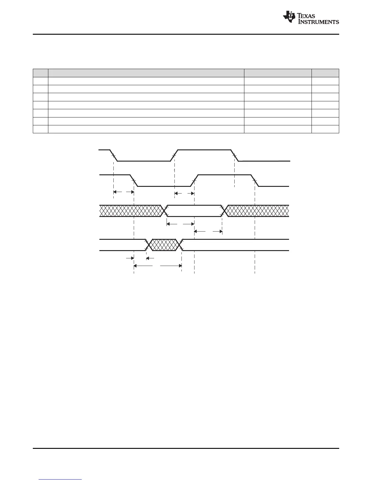
(1) Timings for TDO are specified for a maximum of 50-pF load on TDO.
6.20.5 JTAG Scan Interface Timings
Table 6-36. JTAG Scan Interface Timing
(1)
NO. PARAMETER MIN MAX UNIT
fTCK TCK frequency (at HCLKmax) 12 MHz
fRTCK RTCK frequency (at TCKmax and HCLKmax) 10 MHz
1 td(TCK -RTCK) Delay time, TCK to RTCK 24 ns
2 tsu(TDI/TMS - RTCKr) Setup time, TDI, TMS before RTCK rise (RTCKr) 26 ns
3 th(RTCKr -TDI/TMS) Hold time, TDI, TMS after RTCKr 0 ns
4 th(RTCKr -TDO) Hold time, TDO after RTCKf 0 ns
5 td(TCKf -TDO) Delay time, TDO valid after RTCK fall (RTCKf) 12 ns
Figure 6-15. JTAG Timing
 Loading...


