ZED-F9P-Integration Manual
UBX-18010802 - R02
8 Design Page 98 of 114
Advance Information
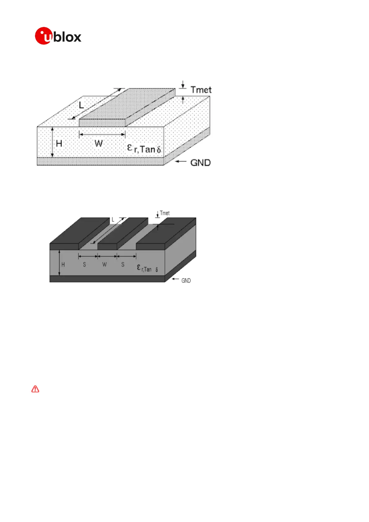
For FR-4 PCB material with a Dielectric permativity of for example 4.7 we can calculate the trace
width at 1575 MHz for 50 Ω impedance.
Figure 72: Microstrip trace width
A grounded co-planar RF trace is recommended as it provides the maximum shielding from noise
with adequate vias to the ground layer.
Figure 73: Grounded coplanar RF trace
Make sure that RF critical circuits are clearly separated from any other digital circuits on the system
board. To achieve this, position the receiver digital part towards your digital section of the system
PCB and have the RF section and antenna placed as far as possible away from the other digital
circuits on the board.
A proper GND concept shall be followed: The RF section should not be subject to noisy digital supply
currents running through its GND plane.
Care must also be exercised with placing the receiver in proximity to circuitry that can emit heat. The
RF part of the receiver is very sensitive to temperature and sudden changes can have an adverse
impact on performance.
Attention :The TCXO of a GNSS receiver is a temperature sensitive device. Avoid high
temperature drift and air convection.
The RF trace must be shielded by vias to Ground along the entire length of the trace and the ZED-
F9P high precision receiver RF_IN pad should be surrounded by vias as shown in the figure below.
 Loading...