56 www.xilinx.com 7 Series FPGAs GTP Transceivers User Guide
UG482 (v1.9) December 19, 2016
Chapter 2: Shared Features
GTP Transceiver RX PMA Reset
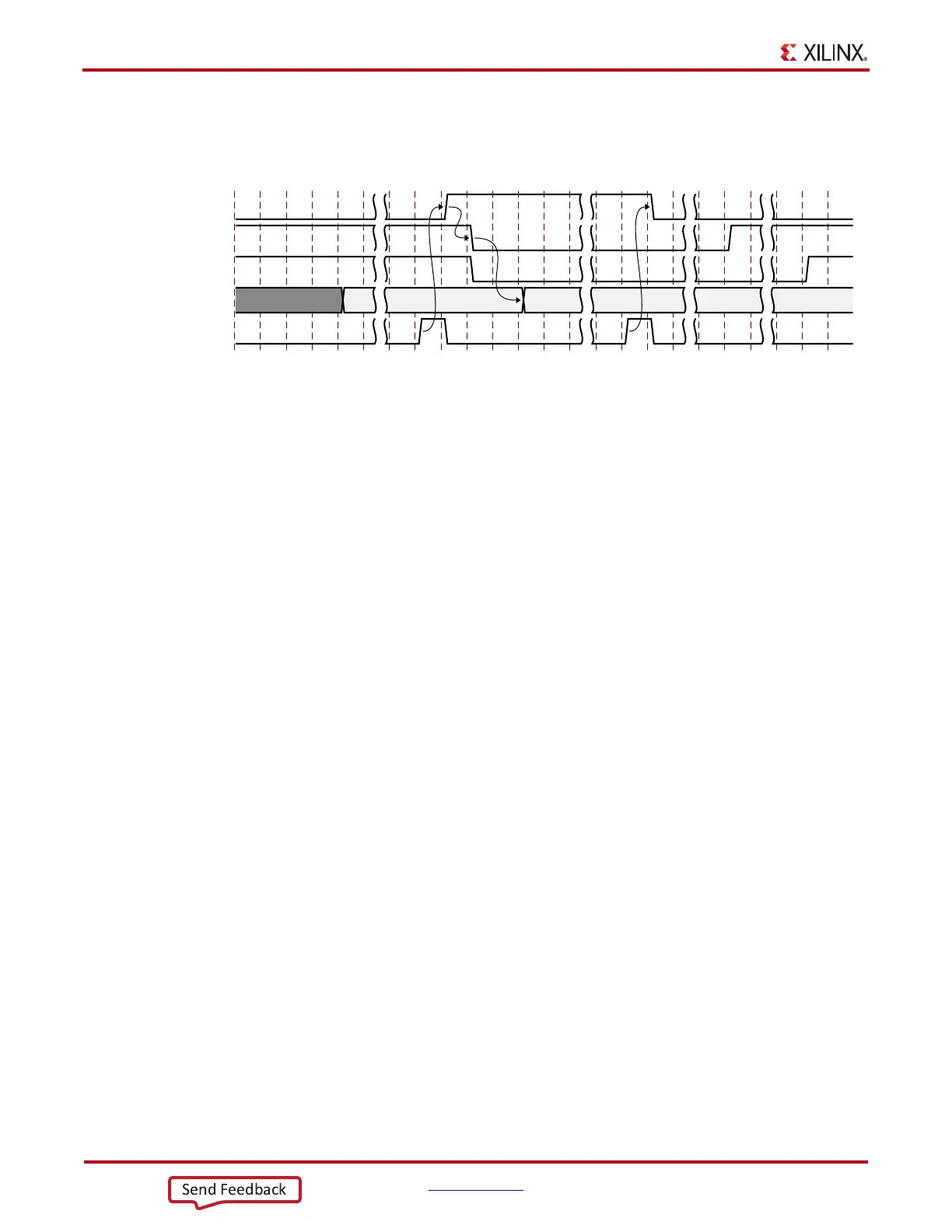
When users want to issue an RXPMARESET, the steps in Figure 2-21 should be performed.
1. “DRP wr” denotes the function of performing a DRP write to addr 9’h011. The exact DRP
transaction is not shown.
2. The sequence of events in Figure 2-21 is not drawn to scale.
3. When the user wants to trigger a RXPMARESET, issue a DRP write to the GTPE2_CHANNEL
primitive, DRPADDR 9‘h011, set bit[11] to 1’b0.
a. To ensure only bit[11] of DRPADDR 9‘h011 is modified, it is best to perform a
read-modify-write function.
4. Upon DRP write completion, set and hold RXPMARESET High.
5. Wait for RXPMARESETDONE to be detected Low.
6. Issue a DRP write to the GTPE2_CHANNEL primitive, DRPADDR 9‘h011, restoring the
original setting for bit[11].
7. Upon DRP write completion, the user can set and hold RXPMARESET Low as desired. The
user can extend the assertion of RXPMARESET, as long as RXPMARESET is held High until
the DRP write is completed.
8. RXPMARESET should be driven with an output of a register to avoid glitches.
GTP Transceiver RX Component Resets
GTP transceiver RX component resets can operate in either sequential mode or single mode. They
are primarily used for special cases. These resets are needed when only a specific subsection needs
to be reset. Table 2-20 and Table 2-21 also summarize all resets available to the GTP transceiver’s
RX and components affected by them in both sequential mode and single mode. These resets are all
asynchronous.
X-Ref Target - Figure 2-21
Figure 2-21: GTP Transceiver RXPMARESET Sequence
UG482_c2_121_020713
RXPMARESET
RXPMARESETDONE
RXRESETDONE
DRP wr(addr ’h011, bit[11])
DRPRDY
1’b0
restore
setting