58 www.xilinx.com 7 Series FPGAs GTP Transceivers User Guide
UG482 (v1.9) December 19, 2016
Chapter 2: Shared Features
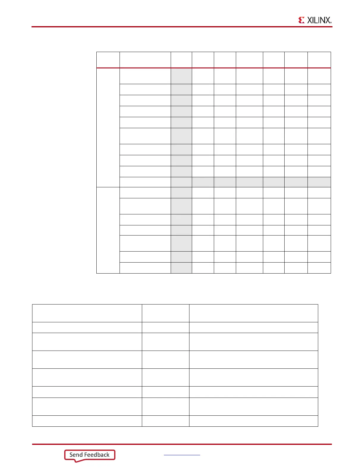
Table 2-22 lists the recommended resets for various situations.
Table 2-21: RX Component Reset Coverage in Single Mode
Functional Blocks
GTRX
RESET
RXPMA
RESET
RXLPM
RESET
EYESCAN
RESET
RXPCS
RESET
RXBUF
RESET
RXOOB
RESET
RX PCS
FPGA RX Fabric
Interface
√
RX Gearbox
√
RX Status Control
√
RX Delay Aligner
√
RX 8B/10B Encoder
√
RX Comma Detect and
Alignment
√
RX Polarity
√
PRBS Checker
√
RX Elastic Buffer
√
RX Reset FSM
RX PMA
RX Analog Front End
√
RX Out-of-Band
Signaling
√√
RX SIPO
√
RX CDR Phase Path
RX CDR Frequency
Path
RX LPM
√
RX ISCAN
√
Table 2-22: Recommended Resets for Common Situations
Situation
Components to
be Reset
Recommended Reset
(1)
After power up and configuration Entire RX GTRXRESET
After turning on a reference clock to the PLL
being used
Entire RX GTRXRESET
After changing the reference clock to the PLL
being used
Entire RX GTRXRESET
After assertion/deassertion of
PLL[0/1]PD, for the PLL being used
Entire RX GTRXRESET
After assertion/deassertion of RXPD[1:0] Entire RX GTRXRESET
RX rate change Entire RX GTRXRESET or reset sequence is performed
automatically due to RXRATE
RX parallel clock source reset RX PCS RXPCSRESET