7 Series FPGAs GTP Transceivers User Guide www.xilinx.com 91
UG482 (v1.9) December 19, 2016
TX Gearbox
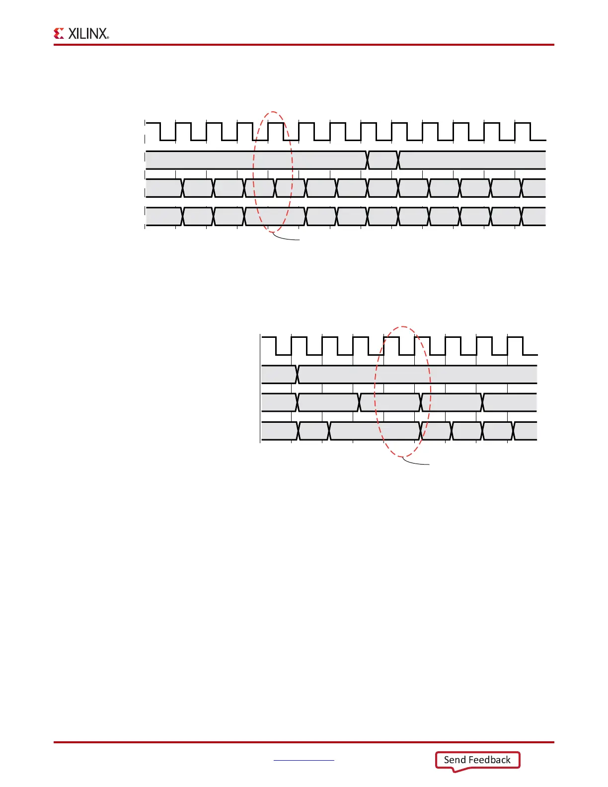
Figure 3-9 shows how a pause occurs at counter value 31 when using an 4-byte fabric interface in
external sequence counter mode with 64B/66B encoding.
Figure 3-10 shows how a pause occurs at counter value 44 when using a 2-byte fabric interface in
external sequence counter mode with 64B/67B encoding.
The sequence of transmitting 64/67 data for the external sequence counter mode is:
1. Apply GTTXRESET and wait until the reset cycle is completed.
2. During reset, apply 7'h00 to TXSEQUENCE, header information to TXHEADER, and initial
data to TXDATA. This state can be held indefinitely until data transmission is ready.
3. On count 0, apply data to TXDATA and header information to TXHEADER. For a 2-byte
interface (TX_DATA_WIDTH = 16), drive the second 2 bytes to TXDATA while still on count
0.
4. The sequence counter increments to 1 while data is driven on TXDATA.
5. After applying 4 bytes of data, the counter increments to 2. Apply data on TXDATA and header
information on TXHEADER.
6. On count 21, stop data pipeline.
7. On count 22, drive data on TXDATA.
8. On count 44, stop data pipeline.
X-Ref Target - Figure 3-9
Figure 3-9: Pause at Sequence Counter Value 31
UG482_c3_09_110911
1
282930313201234567
D
a
D
b
D
c
D
d
D
e
D
f
D
g
D
h
D
i
D
j
D
k
D
l
1
Pause for 1 TXUSRCLK2 cycle.
Data is ignored.
2
TXUSRCLK2
TXHEADER[1:0]
TXSEQUENCE[5:0]
TXDATA[31:0]
X-Ref Target - Figure 3-10
Figure 3-10: Pause at Sequence Counter Value 44
UG482_c3_10_110911
1
42 43 44 45 46
D
a
D
b
D
c
D
d
D
e
D
f
D
g
2
TXUSRCLK2
TXHEADER[2:0]
TXSEQUENCE[6:0]
TXDATA[15:0]
Pause for 2 TXUSRCLK2 cycle.
Data is ignored.