Spartan-3E Starter Kit Board User Guide www.xilinx.com 119
UG230 (v1.0) March 9, 2006
Hirose 100-pin FX2 Edge Connector (J3)
R
Using Differential Outputs
Differential input signals do not require any special voltage. LVDS and RSDS differential
outputs signals, on the other hand, require a 2.5V supply on I/O Bank 0. The board
provides the option to power I/O Bank 0 with either 3.3V or 2.5V. Figure 15-1, page 113
highlights the location of jumper JP9.
If using differential outputs on the FX2 connector, set jumper JP9 to 2.5V. If the jumper is
not set correctly, the outputs switch correctly but the signal levels are out of specification.
UCF Location Constraints
Figure 15-7 provides the UCF constraints for the FX2 connector, including the I/O pin
assignment and the I/O standard used, assuming that all connections use single-ended
I/O standards. These header connections are shared with the 6-pin accessory headers, as
shown in Figure 15-11, page 122.
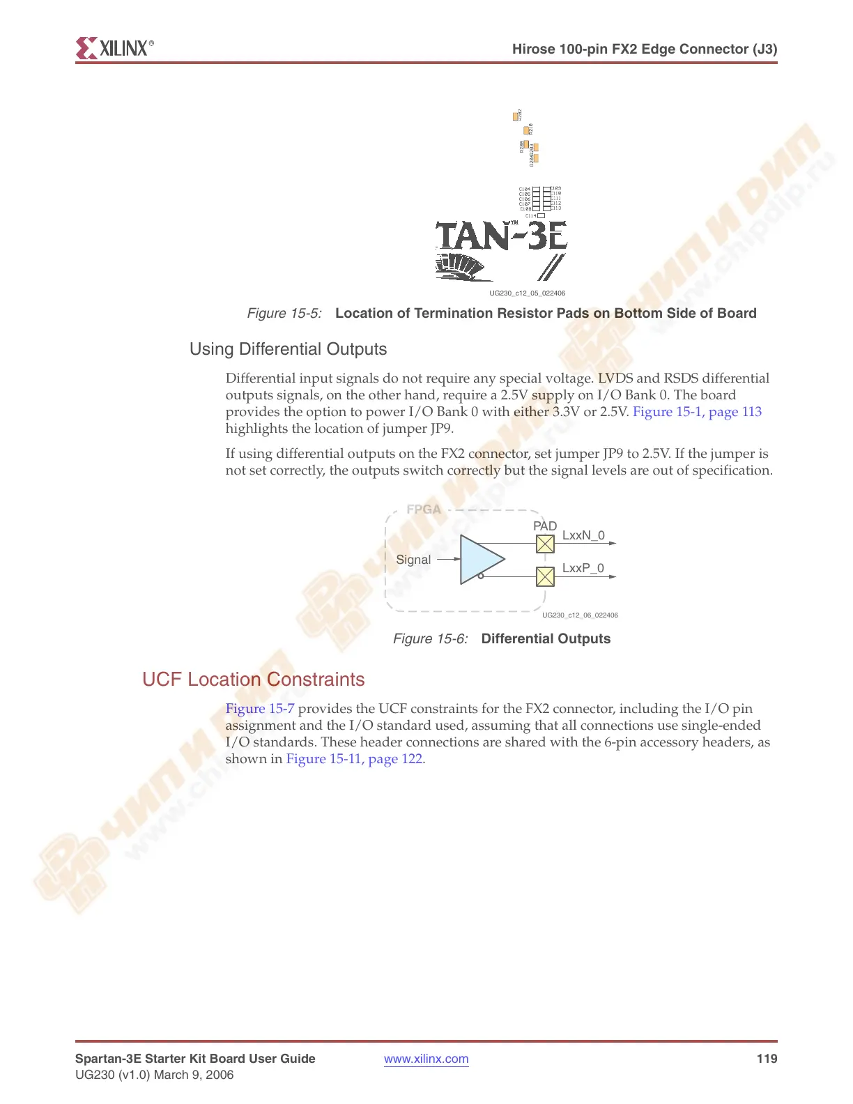
Figure 15-5:
Location of Termination Resistor Pads on Bottom Side of Board
UG230_c12_05_022406
Figure 15-6:
Differential Outputs
LxxN_0
LxxP_0
PA D
Signal
FPGA
UG230_c12_06_022406