74 www.xilinx.com Spartan-3E Starter Kit Board User Guide
UG230 (v1.0) March 9, 2006
Chapter 10:
Analog Capture Circuit
R
Digital Outputs from Analog Inputs
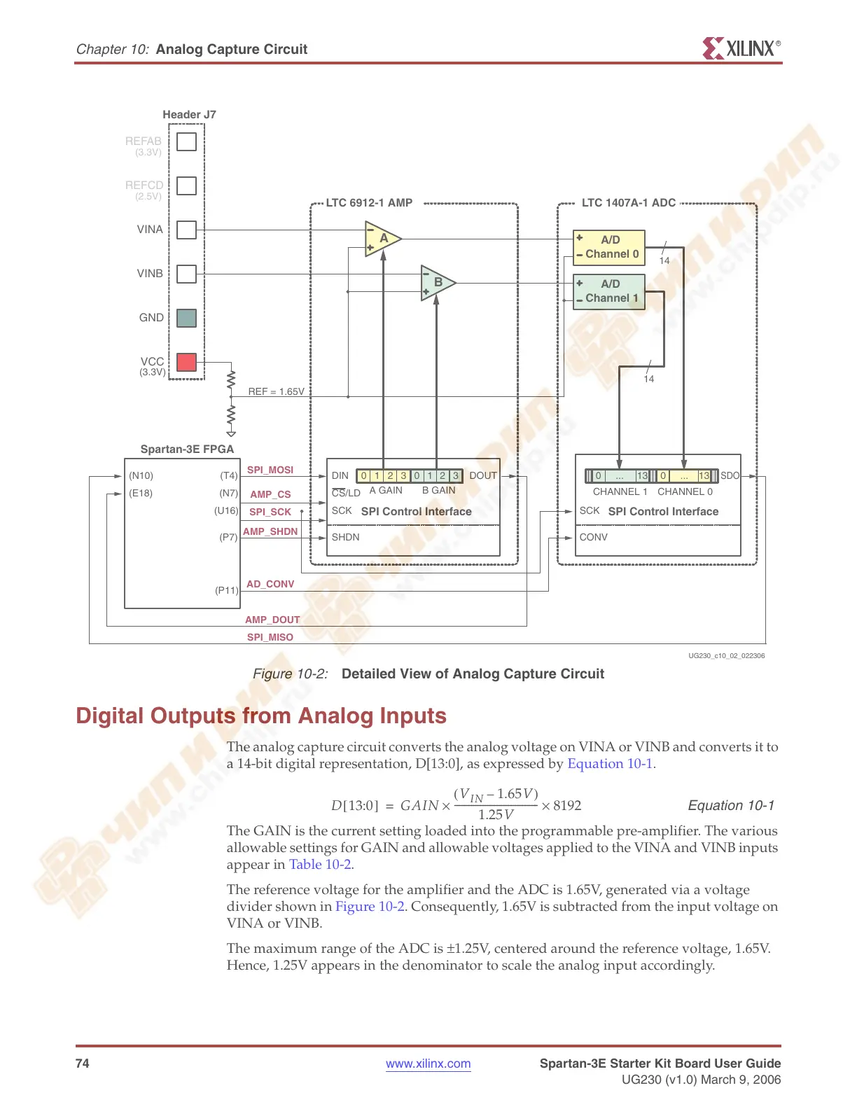
The analog capture circuit converts the analog voltage on VINA or VINB and converts it to
a 14-bit digital representation, D[13:0], as expressed by Equation 10-1.
Equation 10-1
The GAIN is the current setting loaded into the programmable pre-amplifier. The various
allowable settings for GAIN and allowable voltages applied to the VINA and VINB inputs
appear in Table 10-2.
The reference voltage for the amplifier and the ADC is 1.65V, generated via a voltage
divider shown in Figure 10-2. Consequently, 1.65V is subtracted from the input voltage on
VINA or VINB.
The maximum range of the ADC is ±1.25V, centered around the reference voltage, 1.65V.
Hence, 1.25V appears in the denominator to scale the analog input accordingly.
Figure 10-2:
Detailed View of Analog Capture Circuit
Header J7
SPI_MOSI
AMP_CS
SPI_SCK
AMP_SHDN
AMP_DOUT
(N10) (T4)
(U16)
(P7)
(N7)
Spartan-3E FPGA
LTC 6912-1 AMP
REFAB
REFCD
VINA
VINB
GND
VCC
(3.3V)
(3.3V)
(2.5V)
REF = 1.65V
A
B
CS/LD
DIN
SCK
SHDN
DOUT
SPI Control Interface
A GAIN B GAIN
SCK
CONV
SDO
SPI Control Interface
CHANNEL 1 CHANNEL 0
AD_CONV
(P11)
SPI_MISO
(E18)
14
14
LTC 1407A-1 ADC
A/D
Channel 0
A/D
Channel 1
32103210 130 ... 130 ...
UG230_c10_02_022306
D 13:0[]GAIN
V
IN
1.65V–()
1.25V
------------------------------------
× 8192×=