70 www.xilinx.com Spartan-3E Starter Kit Board User Guide
UG230 (v1.0) March 9, 2006
Chapter 9:
Digital to Analog Converter (DAC)
R
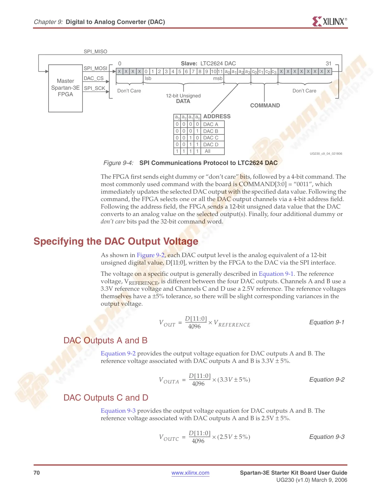
The FPGA first sends eight dummy or “don’t care” bits, followed by a 4-bit command. The
most commonly used command with the board is COMMAND[3:0] = “0011”, which
immediately updates the selected DAC output with the specified data value. Following the
command, the FPGA selects one or all the DAC output channels via a 4-bit address field.
Following the address field, the FPGA sends a 12-bit unsigned data value that the DAC
converts to an analog value on the selected output(s). Finally, four additional dummy or
don’t care bits pad the 32-bit command word.
Specifying the DAC Output Voltage
As shown in Figure 9-2, each DAC output level is the analog equivalent of a 12-bit
unsigned digital value, D[11:0], written by the FPGA to the DAC via the SPI interface.
The voltage on a specific output is generally described in Equation 9-1. The reference
voltage, V
REFERENCE
, is different between the four DAC outputs. Channels A and B use a
3.3V reference voltage and Channels C and D use a 2.5V reference. The reference voltages
themselves have a ±5% tolerance, so there will be slight corresponding variances in the
output voltage.
Equation 9-1
DAC Outputs A and B
Equation 9-2 provides the output voltage equation for DAC outputs A and B. The
reference voltage associated with DAC outputs A and B is 3.3V ± 5%.
Equation 9-2
DAC Outputs C and D
Equation 9-3 provides the output voltage equation for DAC outputs A and B. The
reference voltage associated with DAC outputs A and B is 2.5V ± 5%.
Equation 9-3
Figure 9-4:
SPI Communications Protocol to LTC2624 DAC
310
xxxxxxxx
xxxx
910
a
0
a
1
a
2
a
3
c
0
c
1
c
2
c
3
11876543210
ADDRESS
a
3
a
2
a
1
a
0
0000
0001
0010
0011
All
DAC A
DAC B
DAC C
DAC D
1111
SPI_MOSI
SPI_SCK
DAC_CS
SPI_MISO
12-bit Unsigned
COMMAND
Don’t Care
UG230_c9_04_021806
msblsb
Don’t Care
DATA
Slave: LTC2624 DAC
Master
Spartan-3E
FPGA
V
OUT
D 11:0[]
4096,
-------------------- -
V
REFERENCE
×=
V
OUTA
D 11:0[]
4096,
-------------------- -
3.3V 5%±()×=
V
OUTC
D 11:0[]
4096,
-------------------- -
2.5V 5%±()×=