Spartan-3E Starter Kit Board User Guide www.xilinx.com 43
UG230 (v1.0) March 9, 2006
UCF Location Constraints
R
If the StrataFlash memory is in byte-wide (x8) mode (SF_BYTE = Low), the FPGA
application has full simultaneous read/write access to both the LCD and the StrataFlash
memory. In byte-wide mode, the StrataFlash memory does not use the SF_D<15:8> data
lines.
UCF Location Constraints
Figure 5-2 provides the UCF constraints for the Character LCD, including the I/O pin
assignment and the I/O standard used.
LCD Controller
The 2 x 16 character LCD has an internal Sitronix ST7066U graphics controller that is
functionally equivalent with the following devices.
• Samsung S6A0069X
or KS0066U
• Hitachi HD44780
• SMOS SED1278
Memory Map
The controller has three internal memory regions, each with a specific purpose. The
display must be initialized before accessing any of these memory regions.
DD RAM
The Display Data RAM (DD RAM) stores the character code to be displayed on the screen.
Most applications interact primarily with DD RAM. The character code stored in a DD
RAM location references a specific character bitmap stored either in the predefined CG
ROM character set or in the user-defined CG RAM character set.
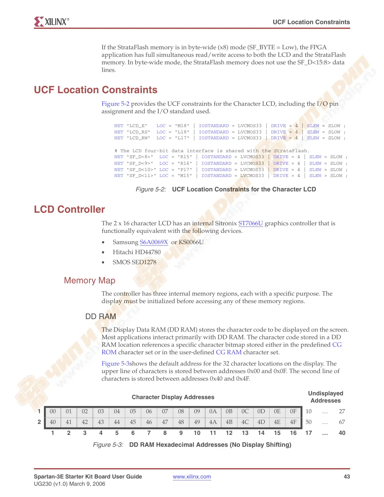
Figure 5-3shows the default address for the 32 character locations on the display. The
upper line of characters is stored between addresses 0x00 and 0x0F. The second line of
characters is stored between addresses 0x40 and 0x4F.
Figure 5-2:
UCF Location Constraints for the Character LCD
NET "LCD_E" LOC = "M18" | IOSTANDARD = LVCMOS33 | DRIVE = 4 | SLEW = SLOW ;
NET "LCD_RS" LOC = "L18" | IOSTANDARD = LVCMOS33 | DRIVE = 4 | SLEW = SLOW ;
NET "LCD_RW" LOC = "L17" | IOSTANDARD = LVCMOS33 | DRIVE = 4 | SLEW = SLOW ;
# The LCD four-bit data interface is shared with the StrataFlash.
NET "SF_D<8>" LOC = "R15" | IOSTANDARD = LVCMOS33 | DRIVE = 4 | SLEW = SLOW ;
NET "SF_D<9>" LOC = "R16" | IOSTANDARD = LVCMOS33 | DRIVE = 4 | SLEW = SLOW ;
NET "SF_D<10>" LOC = "P17" | IOSTANDARD = LVCMOS33 | DRIVE = 4 | SLEW = SLOW ;
NET "SF_D<11>" LOC = "M15" | IOSTANDARD = LVCMOS33 | DRIVE = 4 | SLEW = SLOW ;
Character Display Addresses
Undisplayed
Addresses
1
00 01 02 03 04 05 06 07 08 09 0A 0B 0C 0D 0E 0F 10 … 27
2
40 41 42 43 44 45 46 47 48 49 4A 4B 4C 4D 4E 4F 50 … 67
1234567891011121314151617…40
Figure 5-3:
DD RAM Hexadecimal Addresses (No Display Shifting)