Table 66: RX FEC Ports (cont'd)
Ports Dir Clock Domain Description
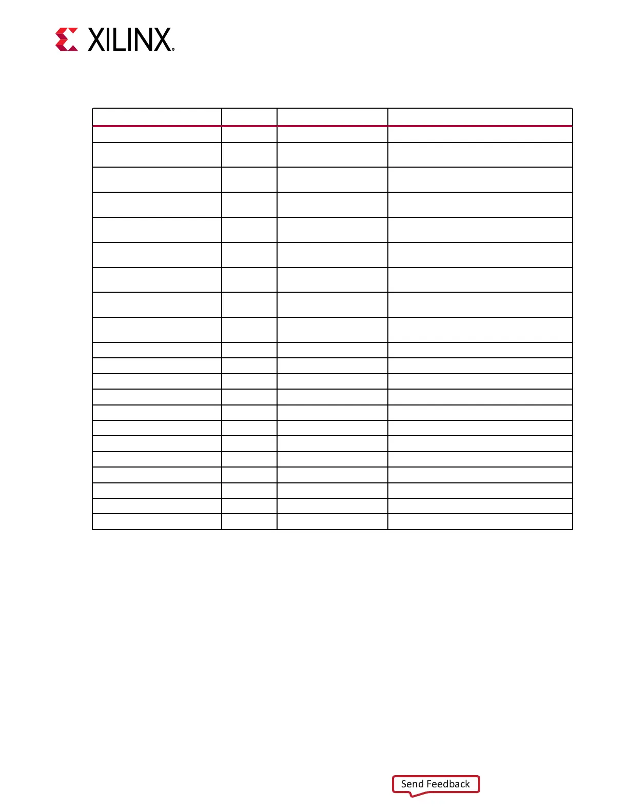
FECTRXLN3LOCK Out CH1_RXUSRCLK2 Lane 3 lock status.
FECRXLN0BITERR0TO1INC[7:0] Out CH0_RXUSRCLK2 Lane 0 bit error count increment (0 corrected
to 1).
FECRXLN1BITERR0TO1INC[7:0] Out CH0_RXUSRCLK2 Lane 1 bit error count increment (0 corrected
to 1).
FECRXLN2BITERR0TO1INC[7:0] Out CH1_RXUSRCLK2 Lane 2 bit error count increment (0 corrected
to 1).
FECRXLN3BITERR0TO1INC[7:0] Out CH1_RXUSRCLK2 Lane 3 bit error count increment (0 corrected
to 1).
FECRXLN0BITERR1TO0INC[7:0] Out CH0_RXUSRCLK2 Lane 0 bit error count increment (1 corrected
to 0).
FECRXLN1BITERR1TO0INC[7:0] Out CH0_RXUSRCLK2 Lane 1 bit error count increment (1 corrected
to 0).
FECRXLN2BITERR1TO0INC[7:0] Out CH1_RXUSRCLK2 Lane 2 bit error count increment (1 corrected
to 0).
FECRXLN3BITERR1TO0INC[7:0] Out CH1_RXUSRCLK2 Lane 3 bit error count increment (1 corrected
to 0).
FECRXLN0ERRCNTINC[3:0] Out CH0_RXUSRCLK2 Lane 0 symbol error count increment.
FECRXLN1ERRCNTINC[3:0] Out CH0_RXUSRCLK2 Lane 1 symbol error count increment.
FECRXLN2ERRCNTINC[3:0] Out CH1_RXUSRCLK2 Lane 2 symbol error count increment.
FECRXLN3ERRCNTINC[3:0] Out CH1_RXUSRCLK2 Lane 3 symbol error count increment.
FECRXLN0MAPPING[1:0] Out CH0_RXUSRCLK2 Logical FEC lane mapped to physical lane 0.
FECRXLN1MAPPING[1:0] Out CH0_RXUSRCLK2 Logical FEC lane mapped to physical lane 1.
FECRXLN2MAPPING[1:0] Out CH1_RXUSRCLK2 Logical FEC lane mapped to physical lane 2.
FECRXLN3MAPPING[1:0] Out CH1_RXUSRCLK2 Logical FEC lane mapped to physical lane 3.
FECRXLN0DLY[14:0] Out CH0_RXUSRCLK2 Lane 0 alignment delay.
FECRXLN1DLY[14:0] Out CH0_RXUSRCLK2 Lane 1 alignment delay.
FECRXLN2DLY[14:0] Out CH1_RXUSRCLK2 Lane 2 alignment delay.
FECRXLN3DLY[14:0] Out CH1_RXUSRCLK2 Lane 3 alignment delay.
The receive poron of the Integrated KP4 RS-FEC operates internally in the CH0_RXUSRCLK
and CH1_RXUSRCLK domains. Data output on CH0_RXDATA is clocked on the rising edge of
CH0_RXUSRCLK2, and data output on CH1_RXDATA is clocked on the rising edge of
CH1_RXUSRCLK2, just as when the FEC is not enabled.
When congured in 100G mode (combined slice 0 and slice 1 operaon), CH0_RXUSRCLK and
CH1_RXUSRCLK must be driven from the same source with low skew. The same applies to
CH0_RXUSRCLK2 and CH1_RXUSRCLK2.
Chapter 4: Receiver
UG581 (v1.0) January 4, 2019 www.xilinx.com
Virtex UltraScale+ GTM Transceivers 108
 Loading...

