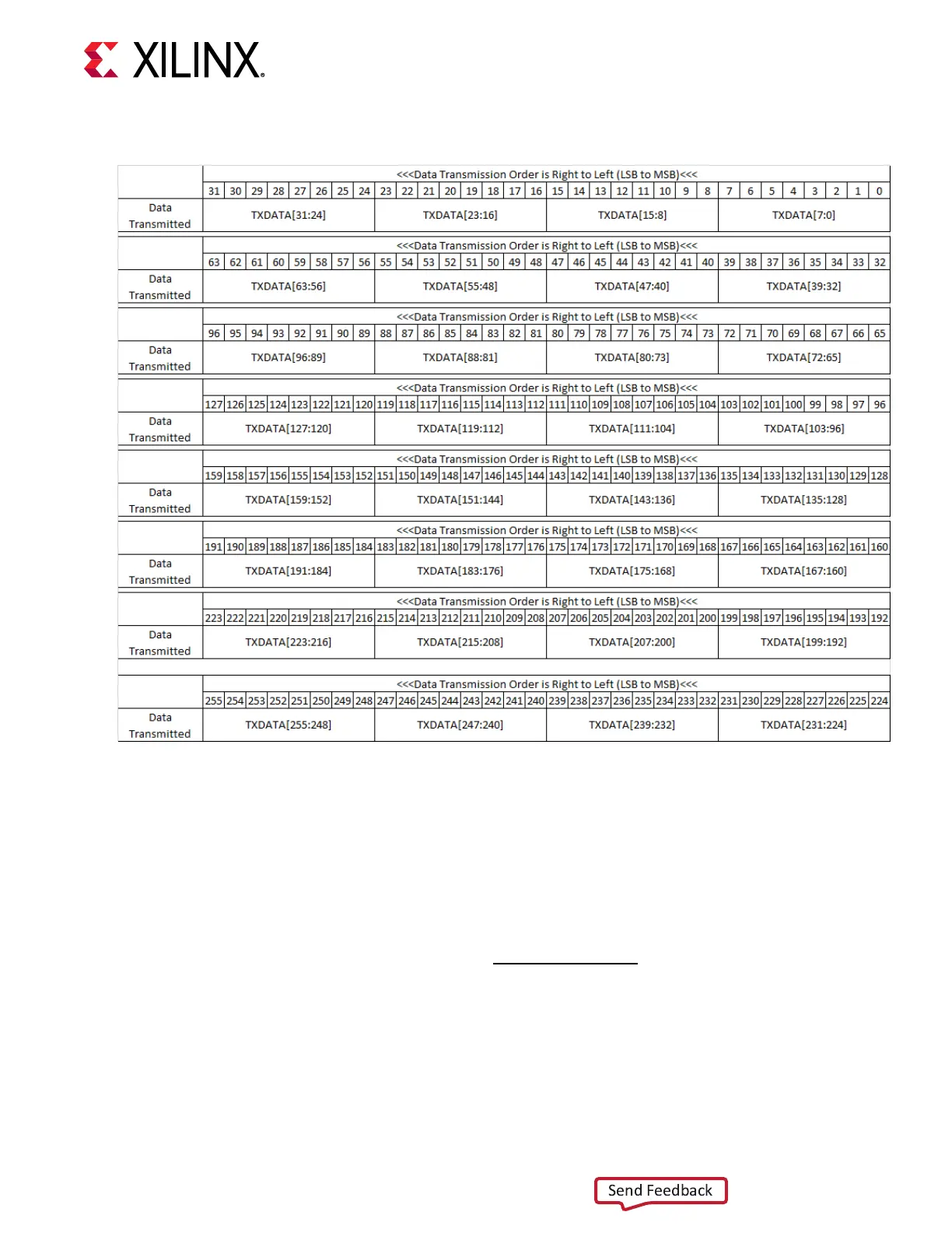
Figure 25: TX Data Transmitted
TXUSRCLK and TXUSRCLK2 Generation
The TX interface includes two parallel clocks: TXUSRCLK and TXUSRCLK2. TXUSRCLK is the
internal clock for the PCS logic in the GTM transmier. The required rate for TXUSRCLK
depends on the internal datapath width of the GTM_DUAL primive and the TX line rate of the
GTM transmier. The following equaon shows how to calculate the required rate for
TXUSRCLK for all cases.
TXUSRCLK Rate =
Line Rate
Internal Datapath Width
Chapter 3: Transmitter
UG581 (v1.0) January 4, 2019 www.xilinx.com
Virtex UltraScale+ GTM Transceivers 56
 Loading...

