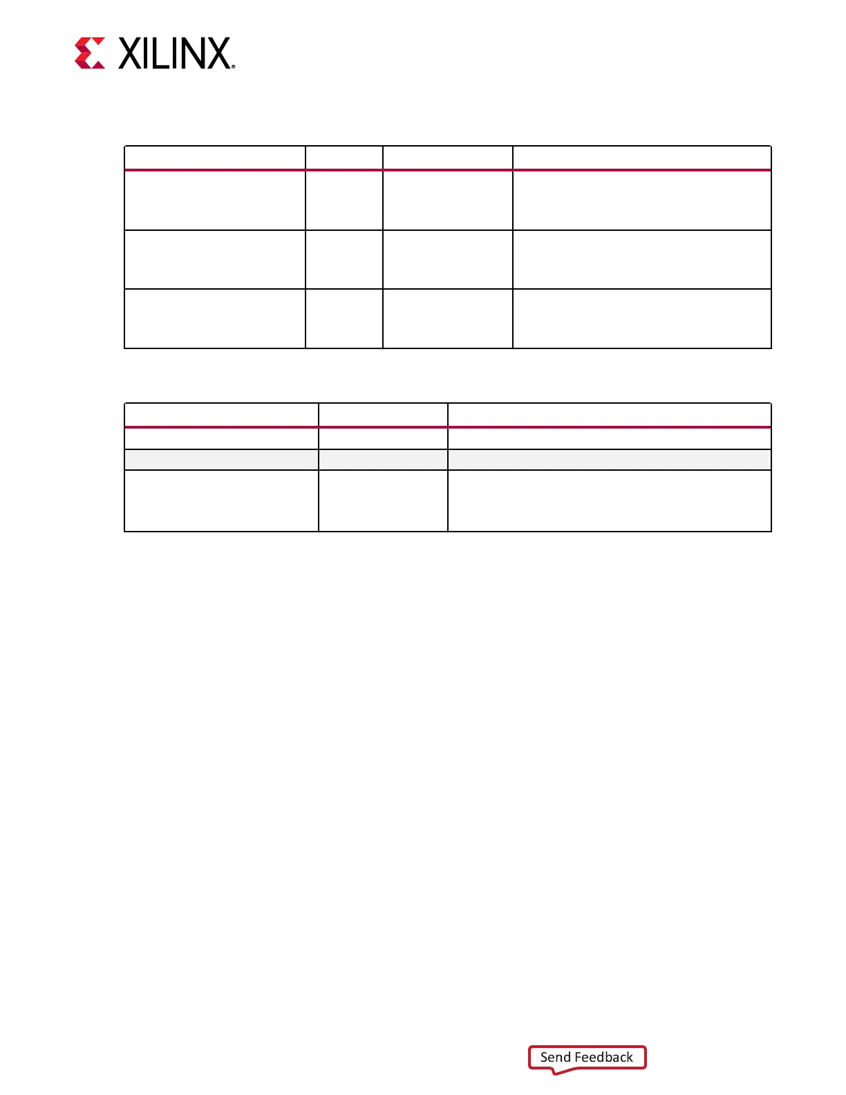
Table 43: TX Programmable Divider Ports
Port Dir Clock Domain Description
CH[0/1]_TXPROGDIVRESET In Async This active-High port resets the dividers as well
as the TXPRGDIVRESETDONE indicator. A reset
must be performed whenever the input clock
source is interrupted.
CH[0/1]_TXPRGDIVRESETDONE Out Async When the input clock is stable and reset is
performed, this active-High signal indicates the
reset is completed and the output clock is
stable.
CH[0/1]_TXPROGDIVCLK Out Clock TXPROGDIVCLK is the parallel clock output from
the TX programmable divider. This clock is the
recommended output to the interconnect logic
through BUFG_GT.
Table 44: TX Programmable Divider Attribute
Attribute Type Description
CH[0/1]_TX_DRV_CFG4 16-bit Reserved.
Bit Name Address Description
TX_PROGDIV_SEL_FULLRATE [15] This attribute is used during the TX programmable divider
ratio selection. Set to 1’b1 to obtain the full rate of the
divided clock. Set to 1’b0 to obtain the half rate of the
divided clock.
Chapter 3: Transmitter
UG581 (v1.0) January 4, 2019 www.xilinx.com
Virtex UltraScale+ GTM Transceivers 75
 Loading...

