ADAV4601 System Design Document Confidential Information
Rev.1 August 2009 Analog Devices Page 13
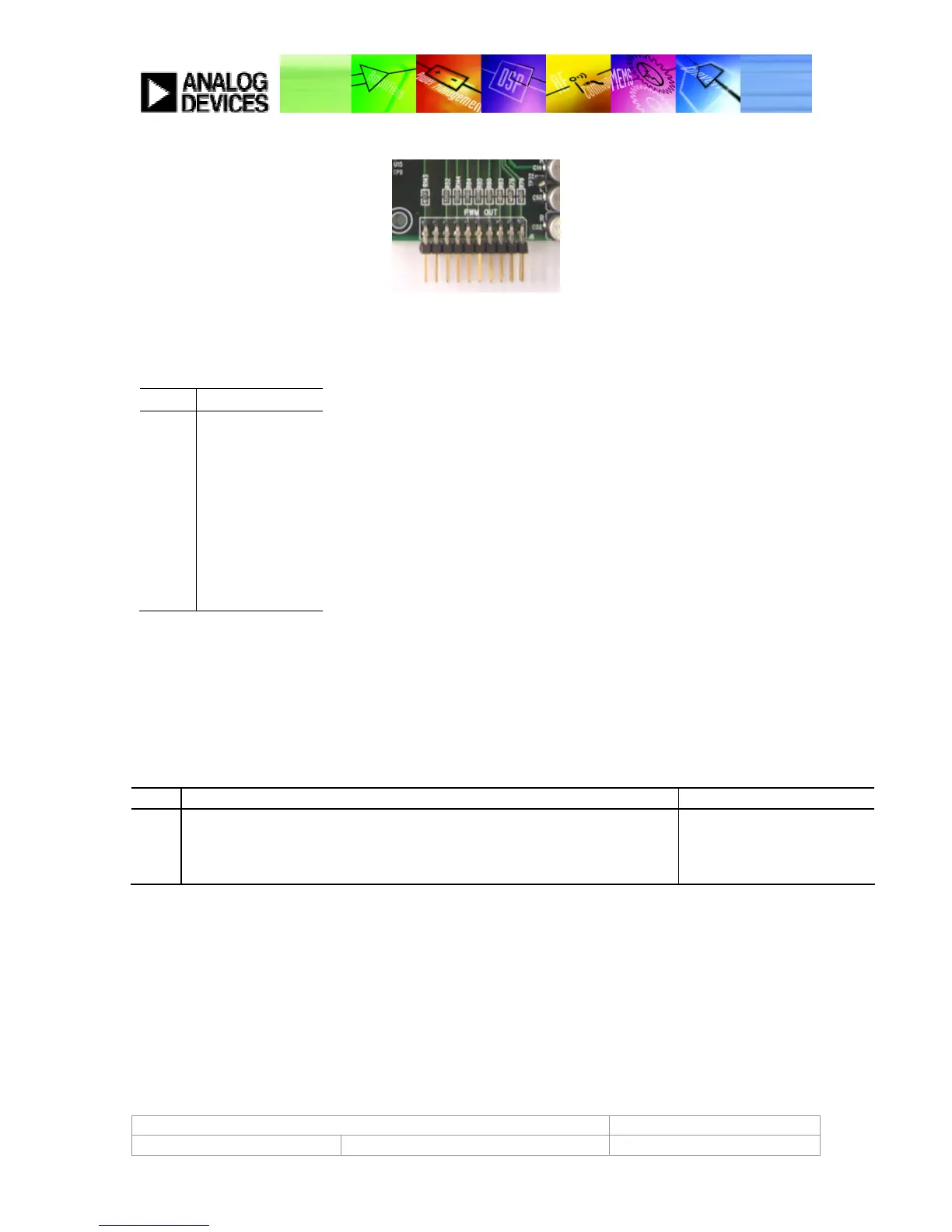
PWM OUTPUTS
Figure 6: PWM Outputs
The differential PWM outputs from the ADAV4601 are available on header J6 for connection to a Class-D power
stage.
Table 3: PWM OUT Signals on J6
Pin Signal
1 PWM4B
3 PWM4A
5 PWM3B
7 PWM3A
9 PWM2B
11 PWM2A
13 PWM1B
15 PWM1A
19 PWM Ready
All other pins are grounded. Please refer to Appendix A – Detailed Register Descriptionsfor more details on register
settings.
LINK/JUMPER CONFIGURATIONS
The links (jumpers) present on the evaluation board are predominantly for in-house evaluation. Table 4below
briefly describes each link.
Table 4: Jumper/Link Configurations
Link Function with jumper in place Comment
LK14
The USB microcontroller U26 is programmable. Should be Out by default.
ADI Evaluation feature only
J17
The EEPROM U15 is writeable.
ADI Evaluation feature only
LK11 Selects if SPDIF from the ADAV4601 or it the converted I2S data from the part is
outputted on the SPDIF transmitter
 Loading...


