Table 4-2 SCC_CFG0 Register bit assignments
Bits Name Function
[31:1] - Reserved. Do not write to these bits.
[0] REMAP_BLOCK_RAM_TO_ZBT This bit remaps block RAM to ZBT:
• 0b0 Does not remap block RAM to ZBT.
• 0b1 Remaps block RAM to ZBT.
Related information
4.3 Register summary on page 4-62
4.4.3 SCC_CFG1 Register
The SCC_CFG1 Register characteristics are:
Purpose
Controls the USER LEDS on the MPS2 and MPS2+ FPGA Prototyping Boards. The MCC polls
this SCC register in the FPGA and updates the appropriate LEDs.
Usage constraints
There are no usage constraints.
Configurations
Available in all MPS2 and MPS2+ configurations.
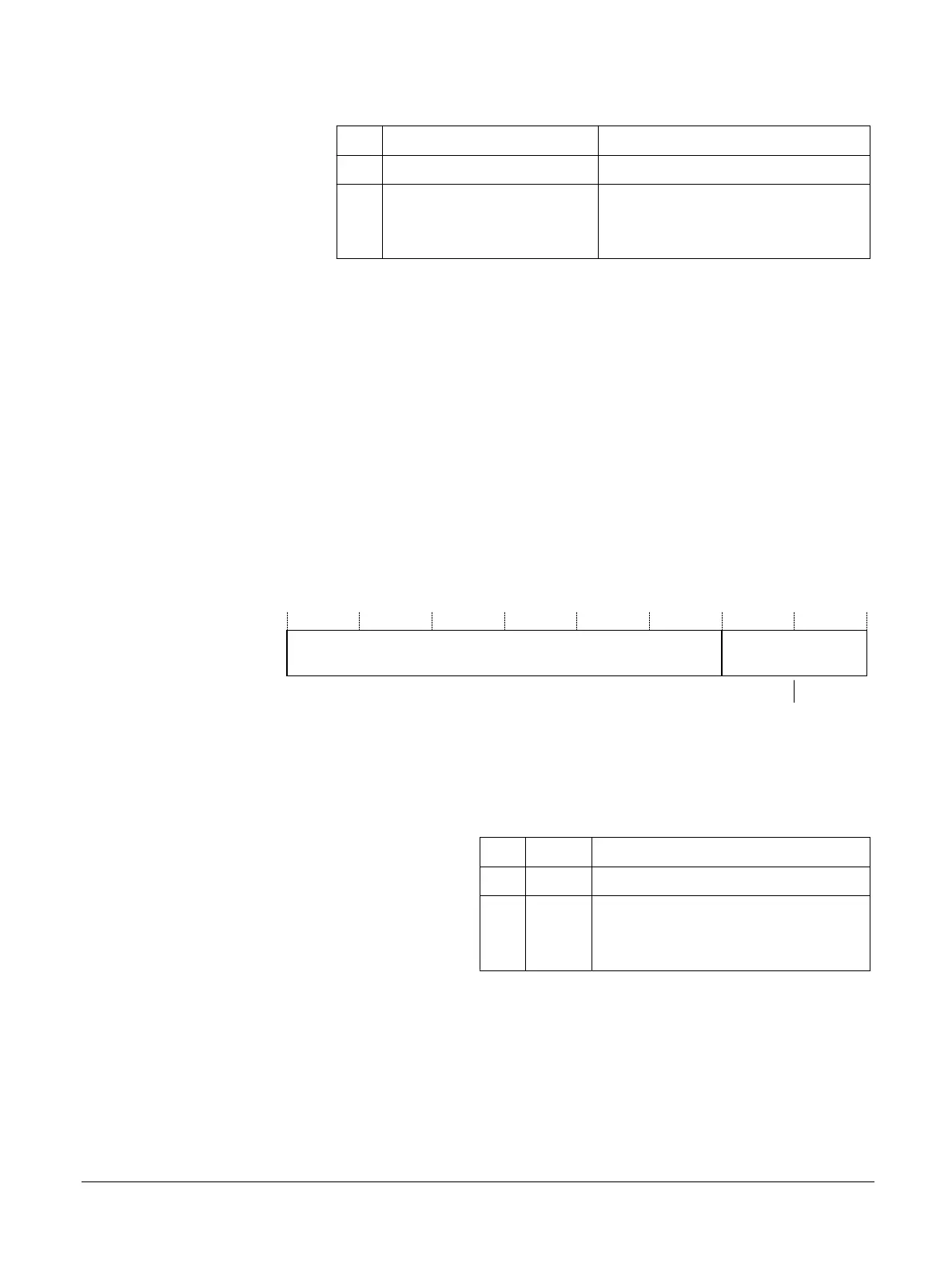
The following figure shows the bit assignments.
31
0
Reserved
LED[7:0]
78
0 0 0
0 0 0 0 0
Figure 4-2 SCC_CFG1 Register bit assignments
The following table shows the bit assignments.
Table 4-3 SCC_CFG1 Register bit assignments
Bits Name Function
[31:8] - Reserved. Do not write to these bits.
[7:0] LED[7:0] These bits control the individual USER LEDs:
• 0b0 Off
• 0b1 On
Related information
2.11 User switches and user LEDs on page 2-35
4.3 Register summary on page 4-62
4.4.4 SCC_CFG3 Register
The SCC_CFG3 Register characteristics are:
4 Programmers Model
4.4 SCC register descriptions
100112_0200_09_en Copyright © 2013–2016, 2018–2020 Arm Limited or its affiliates. All
rights reserved.
4-64
Non-Confidential