5.2 Expansion connectors
The MPS2 and MPS2+ FPGA Prototyping Boards each provide two IDC header connectors that support
user expansion.
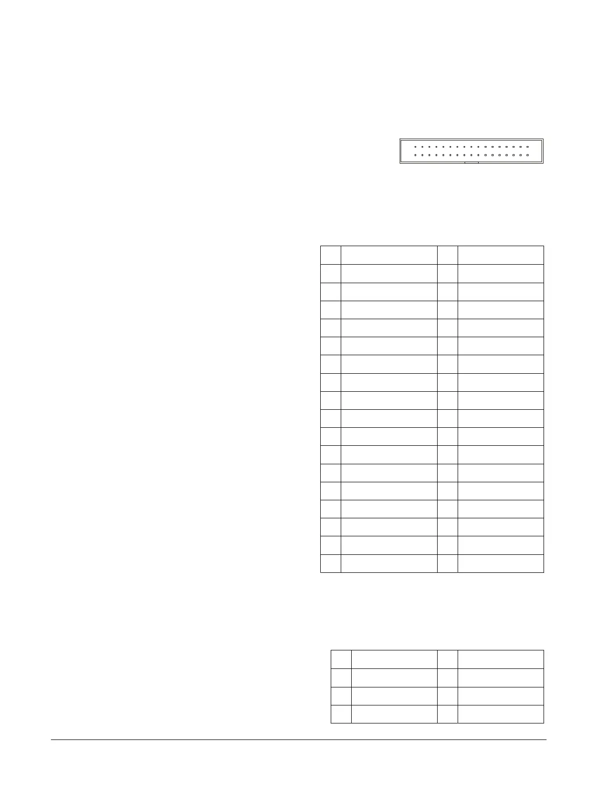
The following figure shows the IDC expansion connector.
1
33
2
34
Figure 5-6 IDC expansion connector
The following two tables show the pin mappings for the IDC expansion connectors EXP1, component
number J7, and EXP2, component number J8, which support general‑purpose I/O expansion.
Table 5-6 Expansion connector EXP1, J7, signal list
Pin Signal Pin Signal
1 EXP0 2 EXP14
3 EXP1 4 EXP15
5 EXP2 6 EXP16
7 EXP3 8 EXP17
9 EXP4 SI Clock output 10 EXP18
11 GND 12 GND
13 EXP5 SI Clock output 14 EXP19 Clock output
15 EXP6 16 EXP20
17 EXP7 18 EXP21
19 EXP8 20 EXP22
21 EXP9 22 EXP23
23 EXP10 24 GND
25 EXP11 SI Clock output 26 3V
27 3V 28 GND
29 GND 30 3V
31 EXP12 32 EXP24
33 EXP13 34 EXP25
Pins 9, 13, 14, and 25 of connector EXP1 have source series terminating resistors. These resistors help to
maintain the integrity of high slew-rate signals. Arm recommends these pins for use as clock outputs or
sensitive data outputs in preference to other pins.
Table 5-7 Expansion connector EXP2, J8, signal list
Pin Signal Pin Signal
1 EXP26 2 EXP40
3 EXP27 4 EXP41
5 EXP28 6 EXP42
5 Signal Descriptions
5.2 Expansion connectors
100112_0200_09_en Copyright © 2013–2016, 2018–2020 Arm Limited or its affiliates. All
rights reserved.
5-80
Non-Confidential